[转帖]AMD Zen CPU 架构以及不同CPU性能大PK
https://plantegg.github.io/2021/08/13/AMD_Zen_CPU%E6%9E%B6%E6%9E%84/
前言
本文先介绍AMD Zen 架构,结合前一篇文章《CPU的生产和概念》一起来看效果会更好,在CPU的生产和概念中主要是以Intel方案来介绍,CPU的生产和概念中的 多核和多个CPU方案2 就是指的AMD Zen2架构。
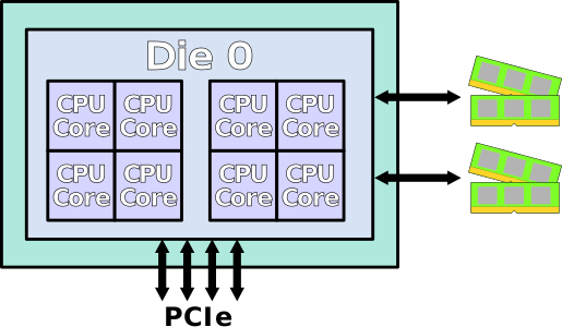
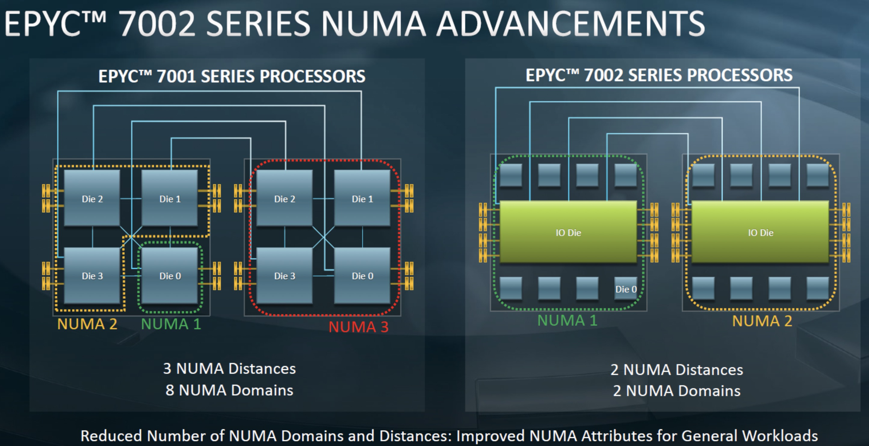
Zen1 和 Intel 还比较像,只是一个CPU会封装多个小的Die来得到多核能力,导致NUMA node比较多。
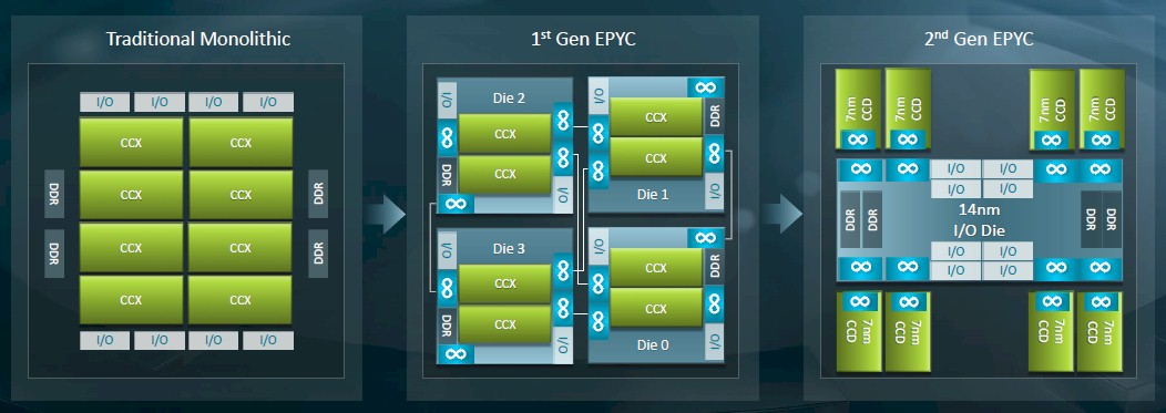
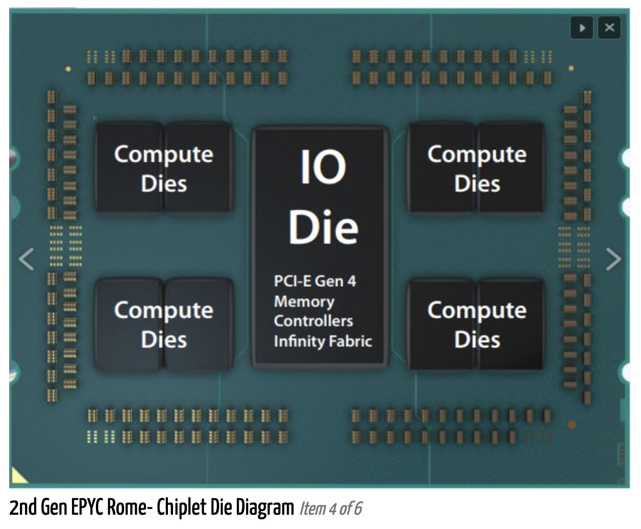
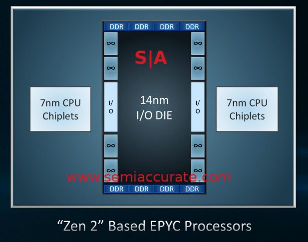
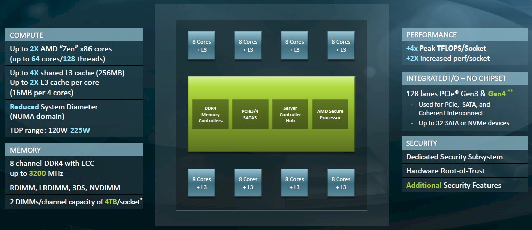
AMD 从Zen2开始架构有了比较大的变化,Zen2架构改动比较大,将IO从Core Die中抽离出来,形成一个专门的IO Die,这个IO Die可以用上一代的工艺实现来提升成品率降低成本。剩下的core Die 专注在core和cache的实现上,同时可以通过最新一代的工艺来提升性能。并且在一个CPU上封装一个 IO Die + 8个 core Die这样一块CPU做到像Intel一样就是一个大NUMA,但是成本低了很多,也许在云计算时代这么搞比较合适。当然会被大家笑话为胶水核(用胶水把多个Die拼在一起),性能肯定是不如一个大Die好,但是挡不住便宜啊。这估计就是大家所说的 AMD YES!吧
比如Core Die用7nm工艺,IO Die用14nm工艺,一块CPU封装8个Core Die+1个IO Die的话既能得到一个多核的CPU成本有非常低,参考 《CPU的生产和概念》中的良品率和成品部分。
介绍完AMD架构后,会拿海光7280这块CPU(实际是OEM的AMD Zen1 架构,一块芯片封装4个die)和 Intel的CPU用MySQL 来对比一下实际性能。
网上Intel CPU架构、技术参数等各种资料还是很丰富的,但是AMD EPYC就比较少了,所以先来学习一下EPYC的架构特点。
AMD EPYC CPU演进路线
后面会针对 第二代的 EPYC来做一个对比测试。
AMD EPYC CPU Families:
| Family Name | AMD EPYC Naples | AMD EPYC Rome | AMD EPYC Milan | AMD EPYC Genoa |
|---|---|---|---|---|
| Family Branding | EPYC 7001 | EPYC 7002 | EPYC 7003 | EPYC 7004? |
| Family Launch | 2017 | 2019 | 2021 | 2022 |
| CPU Architecture | Zen 1 | Zen 2 | Zen 3 | Zen 4 |
| Process Node | 14nm GloFo | 7nm TSMC | 7nm TSMC | 5nm TSMC |
| Platform Name | SP3 | SP3 | SP3 | SP5 |
| Socket | LGA 4094 | LGA 4094 | LGA 4094 | LGA 6096 |
| Max Core Count | 32 | 64 | 64 | 96 |
| Max Thread Count | 64 | 128 | 128 | 192 |
| Max L3 Cache | 64 MB | 256 MB | 256 MB | 384 MB? |
| Chiplet Design | 4 CCD’s (2 CCX’s per CCD),4 Die | 8 CCD’s (2 CCX’s per CCD) + 1 IOD ,9 Die | 8 CCD’s (1 CCX per CCD) + 1 IOD | 12 CCD’s (1 CCX per CCD) + 1 IOD |
| Memory Support | DDR4-2666 | DDR4-3200 | DDR4-3200 | DDR5-5200 |
| Memory Channels | 8 Channel | 8 Channel | 8 Channel | 12 Channel |
| PCIe Gen Support | 64 Gen 3 | 128 Gen 4 | 128 Gen 4 | 128 Gen 5 |
| TDP Range | 200W | 280W | 280W | 320W (cTDP 400W) |
命名规范:
Zen1
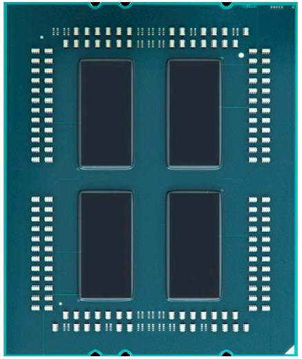
hygon 5280封装后类似下图(一块CPU封装了2个Die,还有封装4个Die的,core更多更贵而已)
或者4个Die封装在一起
Zen1 Die
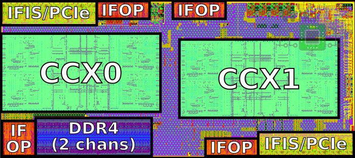
下面这块Die集成了两个CCX(每个CCX四个物理core), 同时还有IO接口
Quad-Zeppelin Configuration, as found in EPYC.
Zen CPU Complex(CCX)
hygon 5280使用这个结构, There are 4 cores per CCX and 2 CCXs per die for 8 cores.
- 44 mm² area
- L3 8 MiB; 16 mm²
- 1,400,000,000 transistors
封装后的Zen1(4Die)
4个Die的内部关系
详实数据和结构
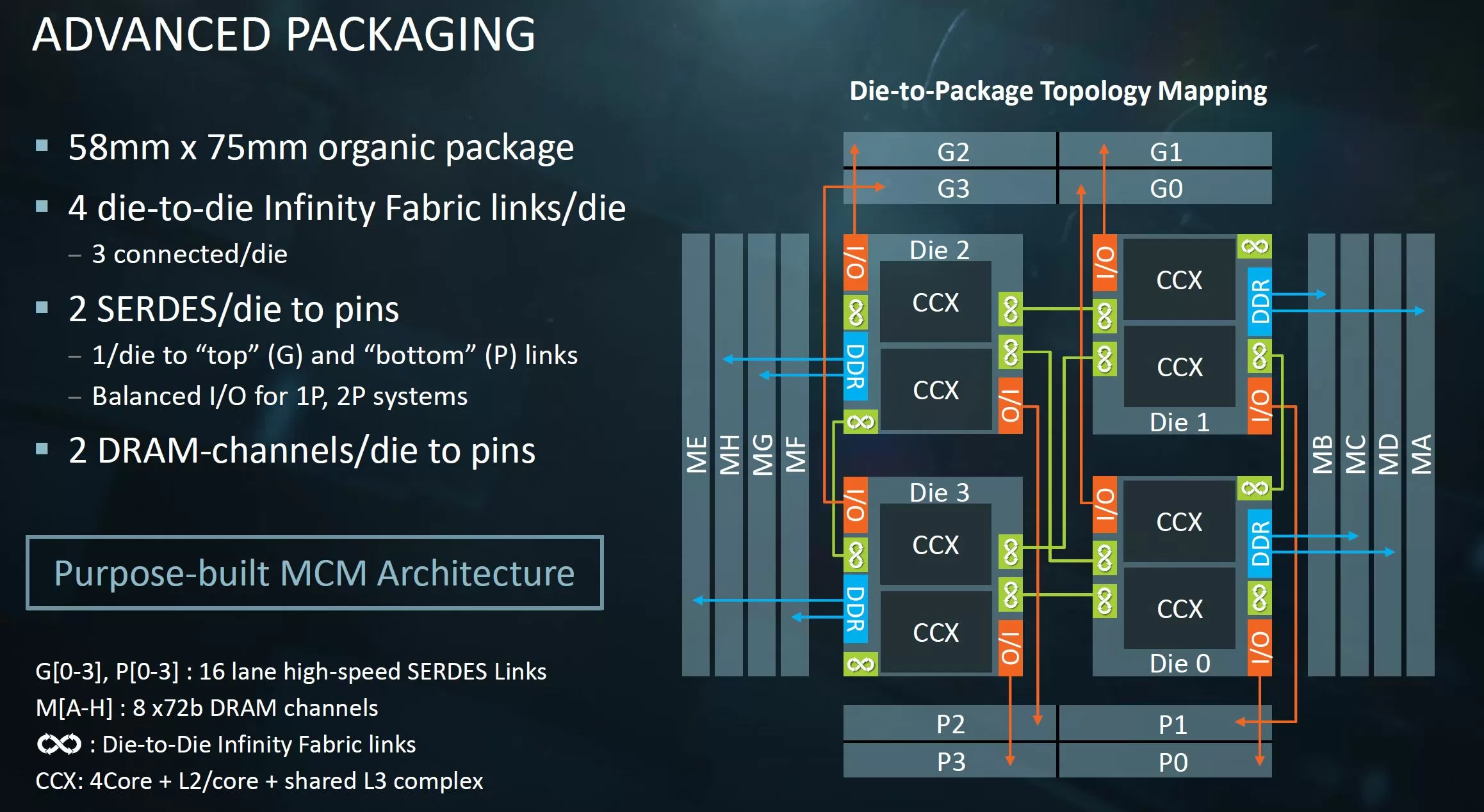
Zen2 Rome
Zen2开始最大的变化就是将IO从Core Die中抽离出来,形成一个专门的IO Die。封装后如下图:
以上结构的CPU在2路服务器下的内部结构:
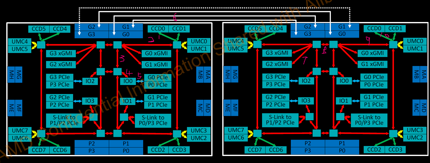
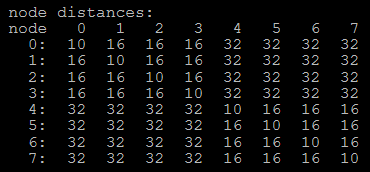
跨socket的内存访问的数据流跟互联有关,如上图标示,比如从左边的CCD0到右边的CCD0的内存,大概需要经过10跳。
| node0 | node1 | node2 | node3 | node4 | node5 | node6 | node7 | |
|---|---|---|---|---|---|---|---|---|
| node0 | 89.67 | 99.357 | 108.11 | 110.54 | 181.85 | 187.71 | 179.507 | 179.463 |
| node1 | 90.983 | 111.65 | 106.11 | 188.77 | 194.7 | 188.179 | 189.512 | |
| node2 | 91.2 | 98.272 | 180.95 | 190.53 | 184.865 | 186.088 | ||
| node3 | 89.971 | 186.81 | 193.43 | 192.459 | 192.615 | |||
| node4 | 89.566 | 97.943 | 108.19 | 109.942 | ||||
| node5 | 90.927 | 111.123 | 108.046 | |||||
| node6 | 91.212 | 103.719 | ||||||
| node7 | 89.692 |
上面表格是3 xGMI互联的情况下,测试出来的访存时延,可以看到在某些node间访存时延会有一些的突增,不够均匀,比如node1到node 5、node2到node5;上述latency跨socket如果用默认BIOS值在280左右
以下表格是厂商默认值和优化值对比(用优化值能将latency从280下降到180左右):
| 参数 | 可选项 | 默认值 (milan:V260 rome:V26.02) | 优化值 | 备注 |
|---|---|---|---|---|
| xGMI Link Width Control | Manual/Auto | Auto | Manual | |
| xGMI Force Link Width Control | Unforce/Force | Unforce | Force | |
| xGMI Force Link Width | 0/1/2 | 2 | 2 | 2 = Force xGMI link width to x16 |
| 3-link xGMI max speed | [00]6.4Gbps …… [0A]16Gbps ……[13]25Gbps *[FF]Auto | Auto | 16Gbps | IEC的rome和milan都是16Gbs,其他产品要与硬件确认 |
另外发现启用透明大页后测试内存时延能降低20%(通过perf发现没开THP的tlb miss很高)
Zen2 Core Complex Die
- TSMC 7-nanometer process
- 13 metal layers[1]
- 3,800,000,000 transistors[2]
- Die size: 74 mm²
- CCX size: 31.3 mm², 4core per CCX // 16M L3 perf CCX
- 2 × 16 MiB L3 cache: 2 × 16.8 mm² (estimated) // 中间蓝色部分是L3 16M,一个Die封装两个CCX的情况下

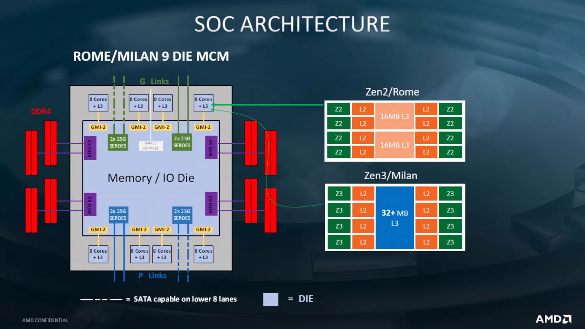
在Zen2/Rome架构中,一个CCD由两个CCX构成,一个CCX包含4个物理核,共享16MB的L3 cache。
在Zen3/Milan架构中,抛弃了两个CCX组成一个CCD的概念,一个CCD直接由8个物理核构成,共享整个Die上的32MB L3 cache。
Zen1 VS Zen2
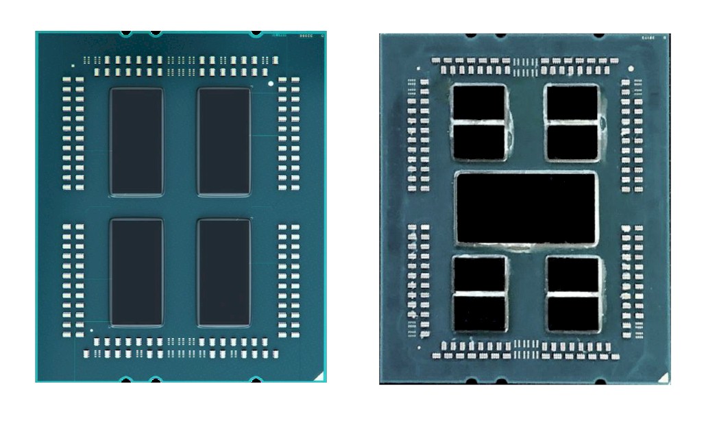
Here is what the Naples and Rome packages look like from the outside:
numa
zen1 numa distance:
hygon numa distance:
|
1
2
3
4
5
6
7
8
9
10
11
12
13
14
15
16
17
18
19
20
21
22
23
24
25
26
27
28
29
30
31
32
33
|
# numactl -H //Zen1 hygon 7280 2 socket enable die interleaving
available: 2 nodes (0-1)
node 0 cpus: 0 1 2 3 4 5 6 7 8 9 10 11 12 13 14 15 16 17 18 19 20 21 22 23 24 25 26 27 28 29 30 31 64 65 66 67 68 69 70 71 72 73 74 75 76 77 78 79 80 81 82 83 84 85 86 87 88 89 90 91 92 93 94 95
node 0 size: 257578 MB
node 0 free: 115387 MB
node 1 cpus: 32 33 34 35 36 37 38 39 40 41 42 43 44 45 46 47 48 49 50 51 52 53 54 55 56 57 58 59 60 61 62 63 96 97 98 99 100 101 102 103 104 105 106 107 108 109 110 111 112 113 114 115 116 117 118 119 120 121 122 123 124 125 126 127
node 1 size: 257005 MB
node 1 free: 221031 MB
node distances:
node 0 1
0: 10 22
1: 22 10
#numactl -H //Zen1 hygon 5280 2 socket disable die interleaving
available: 4 nodes (0-3)
node 0 cpus: 0 1 2 3 4 5 6 7 32 33 34 35 36 37 38 39
node 0 size: 128854 MB
node 0 free: 89350 MB
node 1 cpus: 8 9 10 11 12 13 14 15 40 41 42 43 44 45 46 47
node 1 size: 129019 MB
node 1 free: 89326 MB
node 2 cpus: 16 17 18 19 20 21 22 23 48 49 50 51 52 53 54 55
node 2 size: 128965 MB
node 2 free: 86542 MB
node 3 cpus: 24 25 26 27 28 29 30 31 56 57 58 59 60 61 62 63
node 3 size: 129020 MB
node 3 free: 98227 MB
node distances:
node 0 1 2 3
0: 10 16 28 22
1: 16 10 22 28
2: 28 22 10 16
3: 22 28 16 10
|
看完这些结构上的原理,让我们实际来看看AMD的性能怎么样。
hygon 7280 PCM数据
hygon pcm(performance counter monitor) 工具由芯片公司提供
|
1
2
3
4
5
6
7
8
9
10
11
12
13
14
15
16
17
18
19
20
21
22
23
24
25
26
27
28
29
30
31
32
33
34
35
36
37
38
39
40
41
42
43
44
45
46
47
48
49
50
51
52
53
54
55
56
57
|
[root@hygon3 16:58 /root/PCM]
#./pcm.x -r -topdown -i=1 -nc -ns -l2
Processor Counter Monitor (2019-08-21 17:07:31 +0800 ID=378f2fc)
Number of physical cores: 64
Number of logical cores: 128
Number of online logical cores: 128
Threads (logical cores) per physical core: 2
Num sockets: 2
Physical cores per socket: 32
Core PMU (perfmon) version: 3
Number of core PMU generic (programmable) counters: 6
Width of generic (programmable) counters: 64 bits
Ccxs per Node: 8
Logical cores per Ccx: 8
Physical Cores per Ccx: 4
Nodes per socket: 4
Number of core PMU fixed counters: 0
Width of fixed counters: 0 bits
Nominal core frequency: 2000000000 Hz
Package thermal spec power: -1 Watt; Package minimum power: -1 Watt; Package maximum power: -1 Watt;
Resetting PMU configuration
Zeroed PMU registers
Detected Hygon C86 7280 32-core Processor "Hygon(r) microarchitecture codename DHYANA" stepping 1
EXEC : instructions per nominal CPU cycle
IPC : instructions per CPU cycle
FREQ : relation to nominal CPU frequency='unhalted clock ticks'/'invariant timer ticks' (includes Intel Turbo Boost)
AFREQ : relation to nominal CPU frequency while in active state (not in power-saving C state)='unhalted clock ticks'/'invariant timer ticks while in C0-state' (includes Intel Turbo Boost)
L3MISS: L3 (read) cache misses
L3MPKI: L3 misses per kilo instructions
L3HIT : L3 (read) cache hit ratio (0.00-1.00)
L2DMISS:L2 data cache misses
L2DHIT :L2 data cache hit ratio (0.00-1.00)
L2DMPKI:number of L2 data cache misses per kilo instruction
L2IMISS:L2 instruction cache misses
L2IHIT :L2 instructoon cache hit ratio (0.00-1.00)
L2IMPKI:number of L2 instruction cache misses per kilo instruction
L2MPKI :number of both L2 instruction and data cache misses per kilo instruction
Core (SKT) | EXEC | IPC | FREQ | AFREQ | L2DMISS| L2DHIT | L2DMPKI| L2IMISS| L2IHIT | L2IMPKI| L2MPKI | L3MISS | L3MPKI | L3HIT | TEMP
---------------------------------------------------------------------------------------------------------------
TOTAL * 1.29 1.20 1.08 1.00 12 M 0.73 0.04 10 M 0.87 0.03 0.07 19 M 0.00 0.55 N/A
Instructions retired: 336 G ; Active cycles: 281 G ; Time (TSC): 2082 Mticks ; C0 (active,non-halted) core residency: 107.90 %
PHYSICAL CORE IPC : 2.39 => corresponds to 34.14 % utilization for cores in active state
Instructions per nominal CPU cycle: 2.58 => corresponds to 36.84 % core utilization over time interval
---------------------------------------------------------------------------------------------------------------
Cleaning up
Zeroed PMU registers
|
在本地启动benchmarksql压力,并将进程绑定到0-8core,然后采集到数据:
|
1
2
3
4
5
6
7
8
9
10
11
12
13
14
15
16
17
18
19
20
21
22
23
24
25
26
27
28
29
30
31
32
33
34
35
36
37
38
39
40
41
42
43
44
45
46
47
48
49
50
51
52
53
54
55
56
57
58
59
60
61
62
63
64
65
66
67
68
69
70
71
72
73
74
|
#./pcm.x -r -topdown -i=1 -l2
Processor Counter Monitor (2019-08-21 17:07:31 +0800 ID=378f2fc)
Number of physical cores: 64
Number of logical cores: 128
Number of online logical cores: 128
Threads (logical cores) per physical core: 2
Num sockets: 2
Physical cores per socket: 32
Core PMU (perfmon) version: 3
Number of core PMU generic (programmable) counters: 6
Width of generic (programmable) counters: 64 bits
Ccxs per Node: 8
Logical cores per Ccx: 8
Physical Cores per Ccx: 4
Nodes per socket: 4
Number of core PMU fixed counters: 0
Width of fixed counters: 0 bits
Nominal core frequency: 2000000000 Hz
Package thermal spec power: -1 Watt; Package minimum power: -1 Watt; Package maximum power: -1 Watt;
Resetting PMU configuration
Zeroed PMU registers
Detected Hygon C86 7280 32-core Processor "Hygon(r) microarchitecture codename DHYANA" stepping 1
EXEC : instructions per nominal CPU cycle
IPC : instructions per CPU cycle
FREQ : relation to nominal CPU frequency='unhalted clock ticks'/'invariant timer ticks' (includes Intel Turbo Boost)
AFREQ : relation to nominal CPU frequency while in active state (not in power-saving C state)='unhalted clock ticks'/'invariant timer ticks while in C0-state' (includes Intel Turbo Boost)
L3MISS: L3 (read) cache misses
L3MPKI: L3 misses per kilo instructions
L3HIT : L3 (read) cache hit ratio (0.00-1.00)
L2DMISS:L2 data cache misses
L2DHIT :L2 data cache hit ratio (0.00-1.00)
L2DMPKI:number of L2 data cache misses per kilo instruction
L2IMISS:L2 instruction cache misses
L2IHIT :L2 instructoon cache hit ratio (0.00-1.00)
L2IMPKI:number of L2 instruction cache misses per kilo instruction
L2MPKI :number of both L2 instruction and data cache misses per kilo instruction
Core (SKT) | EXEC | IPC | FREQ | AFREQ | L2DMISS| L2DHIT | L2DMPKI| L2IMISS| L2IHIT | L2IMPKI| L2MPKI | L3MISS | L3MPKI | L3HIT | TEMP
0 0 1.34 1.26 1.06 1.00 8901 K 0.72 3.15 15 M 0.68 5.43 8.58 71 M 4.00 0.60 N/A
1 0 1.42 1.33 1.06 1.00 8491 K 0.73 2.83 14 M 0.68 4.67 7.50 71 M 4.00 0.60 N/A
2 0 1.41 1.33 1.06 1.00 8206 K 0.74 2.75 12 M 0.72 4.25 7.00 71 M 4.00 0.60 N/A
3 0 1.46 1.38 1.06 1.00 7464 K 0.75 2.40 11 M 0.68 3.81 6.21 71 M 4.00 0.60 N/A
4 0 1.31 1.24 1.06 1.00 9118 K 0.71 3.28 15 M 0.69 5.61 8.88 70 M 4.00 0.61 N/A
5 0 1.41 1.33 1.06 1.00 8700 K 0.74 2.92 13 M 0.69 4.66 7.57 70 M 4.00 0.61 N/A
6 0 1.41 1.33 1.06 1.00 8094 K 0.74 2.79 12 M 0.70 4.40 7.18 70 M 4.00 0.61 N/A
7 0 1.43 1.35 1.06 1.00 7873 K 0.74 2.68 12 M 0.71 4.13 6.81 70 M 4.00 0.61 N/A
8 0 1.44 1.36 1.06 1.00 8544 K 0.73 2.79 14 M 0.67 4.87 7.66 20 M 1.00 0.61 N/A
9 0 1.24 1.16 1.06 1.00 524 K 0.51 0.21 86 K 0.94 0.03 0.24 20 M 1.00 0.61 N/A
10 0 1.26 1.18 1.07 1.00 379 K 0.50 0.15 60 K 0.95 0.02 0.17 20 M 1.00 0.61 N/A
11 0 1.24 1.16 1.07 1.00 533 K 0.50 0.20 96 K 0.94 0.04 0.24 20 M 1.00 0.61 N/A
12 0 1.22 1.14 1.07 1.00 1180 K 0.34 0.47 98 K 0.94 0.04 0.51 3872 K 0.12 0.46 N/A
13 0 1.24 1.16 1.07 1.00 409 K 0.49 0.16 64 K 0.94 0.03 0.19 3872 K 0.12 0.46 N/A
---------------------------------------------------------------------------------------------------------------
SKT 0 1.18 1.11 1.06 1.00 113 M 0.67 0.73 139 M 0.71 0.89 1.62 186 M 1.12 0.59 N/A
SKT 1 1.23 1.14 1.08 1.00 33 M 0.53 0.21 11 M 0.89 0.07 0.28 38 M 0.12 0.45 N/A
---------------------------------------------------------------------------------------------------------------
TOTAL * 1.21 1.13 1.07 1.00 147 M 0.65 0.46 150 M 0.74 0.47 0.93 224 M 0.62 0.57 N/A
Instructions retired: 319 G ; Active cycles: 283 G ; Time (TSC): 2108 Mticks ; C0 (active,non-halted) core residency: 107.12 %
PHYSICAL CORE IPC : 2.25 => corresponds to 32.18 % utilization for cores in active state
Instructions per nominal CPU cycle: 2.41 => corresponds to 34.48 % core utilization over time interval
---------------------------------------------------------------------------------------------------------------
Cleaning up
Zeroed PMU registers
|
Apple M1
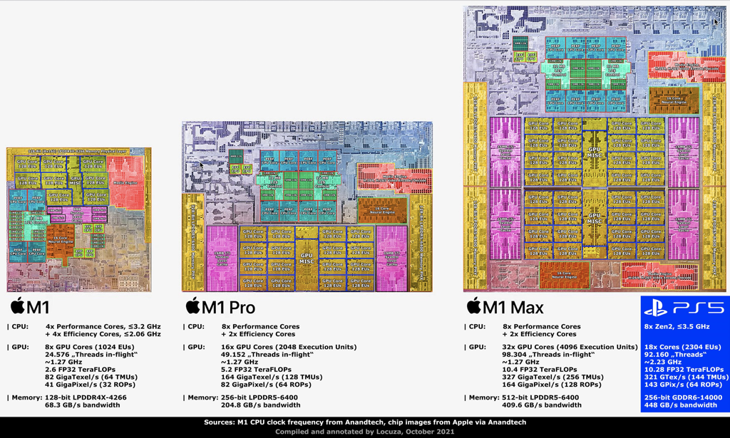
The M1
The critically-acclaimed M1 processor delivers:
- 16 billion transistors and a 119mm squared-die size.
- 4 performance cores, 12MB L2 Cache.
- 4 efficiency cores ith 4MB L2 cache.
- 8 GPU Cores.
- 16GB DDR4x memory at 68GB/s.
The M1 Pro
The M1 Pro takes this higher, with:
- 33.7 billion transistors on a 240mm squared die.
- 8 performance cores, 24MB L2 Cache.
- 2 efficiency cores with 4MB L2 cache.
- 16 GPU Cores.
- 32GB DDR5 memory at 200GB/s.
对比下 i9-12000,i9也有GPU只是没有说多少个,它的GPU频率在0.3到1.55GHz之间
| ISA | x86-64 (x86) |
|---|---|
| Microarchitecture | Alder Lake, Golden Cove, Gracemont |
| Process | Intel 7 |
| Die | 215.25 mm²” 20.5 mm × 10.5 mm |
| MCP | No (1 dies) |
| Cores | 16 |
| Threads | 24 |
| l1$ size | 0.75 MiB (768 KiB, 786,432 B, 7.324219e-4 GiB) + and 0.625 MiB (640 KiB, 655,360 B, 6.103516e-4 GiB) + |
| l1d$ size | 0.25 MiB (256 KiB, 262,144 B, 2.441406e-4 GiB) + and 0.375 MiB (384 KiB, 393,216 B, 3.662109e-4 GiB) + |
| l1i$ size | 0.5 MiB (512 KiB, 524,288 B, 4.882812e-4 GiB) + and 0.25 MiB (256 KiB, 262,144 B, 2.441406e-4 GiB) + |
| l2$ size | 4 MiB (4,096 KiB, 4,194,304 B, 0.00391 GiB) + and 10 MiB (10,240 KiB, 10,485,760 B, 0.00977 GiB) + |
| l3$ size | 6 MiB (6,144 KiB, 6,291,456 B, 0.00586 GiB) + and 24 MiB (24,576 KiB, 25,165,824 B, 0.0234 GiB) + |
The M1 Max
The M1 Max provides:
- 57 billion transistors on a 420mm squared die.
- 8 performance cores, 24MB L2 Cache.
- 2 efficiency cores with 4MB L2 cache.
- 32 GPU Cores.
- 64GB DDR5 memory at 400GB/s.
And the new M1 Ultra
The M1 Ultra brings you:
- 114 billion transistors on a 840mm squared die.
- 16 performance cores, 48MB L2 Cache.
- 4 efficiency cores with 4MB L2 cache.
- 64 GPU Cores.
- Up to 128GB DDR5 memory at 800GB/s.
倚天710
一个die有64core,每两个core是一个cluster,一块cpu封装两个die
一个die大小是314平方毫米,600亿晶体管
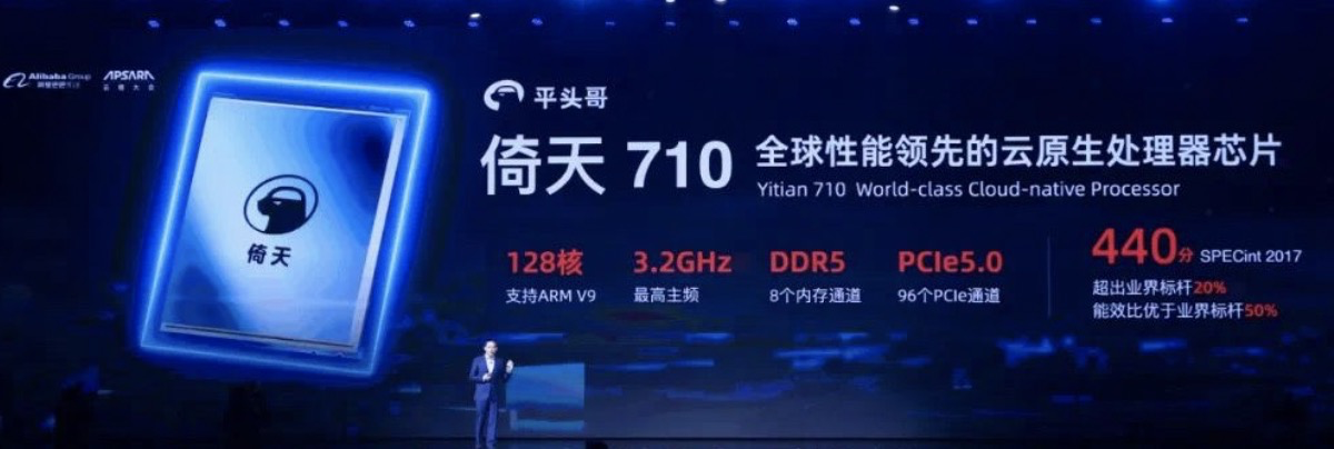
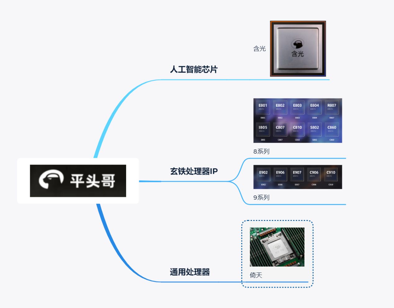
平头哥的几款芯片:
总结
AMD和Intel在服务器领域CPU设计上走了两个不同的方向,Intel通过RingBus、Mesh等方案在一块Die上集成多个core,成本高,在多核场景下性能好。
AMD则是通过设计小的Die来降低成本,然后将多个Die封装到一块CPU上来售卖,Zen1架构的多个Die之间延迟高,于是Zen2将IO抽离出来用一块单独的IO Die来负责IO,这样多核之间的时延比Zen1好了很多。
而在云计算场景下AMD的设计非常有竞争优势,因为云计算大部分时候是要把一块大的CPU分拆售卖,从架构上AMD对分拆售卖非常友好。
整体来说AMD用领先了一代的工艺(7nm VS 14nm),在MySQL查询场景中终于可以接近Intel了,但是海光、鲲鹏、飞腾还是不给力。
参考资料
飞腾ARM芯片(FT2500)的性能测试的性能测试/)
[转帖]AMD Zen CPU 架构以及不同CPU性能大PK的更多相关文章
- [转帖]AMD Zen霄龙中国版:海光x86拿下加解密全球第一
AMD Zen霄龙中国版:海光x86拿下加解密全球第一 http://www.eetop.cn/cpu_soc/6946203.html 其实技术发展都是先模仿 剽窃 再自我创新的 要加以鼓励 总比 ...
- 计算机二进制表示、cpu架构(x86_64)、cpu频率、核心、主板
计算机二进制表示 色彩二进制表示: 红色 255,0,0绿色 0,255,0蓝色 0,0,255 文字二进制表示:A 65a 97 cpu架构 cpu架构有精简指令集和复杂指令集两种精简指令集cpu有 ...
- 手机CPU架构体系分类及各大厂商
手机cpu相关知识,这对于开发Android应用程序适应各个机型有一定的辅助作用 . 手机cpu架构体系分类 指令集可分为复杂指令集(CISC)和精简指令集(RISC)两部分,代表架构分别是x86.A ...
- Linux 4.21包含对AMD Rome处理器中新的Zen 2架构重要的新优化
导读 Phoronix的Linux爱好者报告说,Linux 4.21里包含对AMD Rome处理器中新的Zen 2架构重要的新优化.AMD新推出的7nm EPYC Rome芯片带来了一种全新的独特架构 ...
- 【转帖】AMD Zen之父、Intel副总Jim Keller到底有多牛?
AMD Zen之父.Intel副总Jim Keller到底有多牛? https://www.cnbeta.com/articles/tech/907295.htm 几乎玩过 所有的中国国产化CPU的祖 ...
- [Linux]CPU架构/指令集:RISC / CISC | arm | amd | X86/i386 | aarch64
1 前言 本文是解决在软件开发.软件交付过程中,常常需要找寻与服务器硬件的CPU架构适配的软件包时,开发者和交付者又时常摸不着头脑.[迷迷糊糊]地就下载了某个所谓"适配".&quo ...
- [转帖]AMD、英特尔为何争相走向胶水多核处理器?真相在此
AMD.英特尔为何争相走向胶水多核处理器?真相在此 胶水多核到底好不好?这个事不是简单一句话能说明的,今天的超能课堂里我们就来聊聊MCM胶水多核技术的过去及未来. 作者:孟宪瑞来源:超能网|2018- ...
- 【转帖】龙芯将两款 CPU 核开源,这意味着什么?
龙芯将两款 CPU 核开源,这意味着什么? https://www.oschina.net/news/78316/loongson-open-source-two-cpu-core 文章挺不错的 也讲 ...
- [转帖]AMD第三代锐龙处理器首发评测:i9已无力招架
AMD第三代锐龙处理器首发评测:i9已无力招架 Intel 从之前的 CCX 到了 CCD 增加了缓存 改善了 ccx 之间的延迟. https://baijiahao.baidu.com/s?id= ...
- ios framework 分离与合并多种CPU架构,分离与合并模拟器与真机
ios framework 分离与合并多种CPU架构,分离与合并模拟器与真机 如果你所用的framework支持真机和模拟器多种CPU架构,而你需要的是其中的一种或几种,那么可以可以从framewo ...
随机推荐
- 动态规划问题(四)最长双音序列长度(LBS)
问题描述 以一个乱序的数组,求它的最长双音序列长度.双音序列指该序列先递增,再递减. 如: 对于序列 {1, 11, 2, 10, 4, 5, 2, 1},它的最长双音序列长度为 6, 对于序 ...
- mysql 数据库 定时 备份到阿里云盘
仓库地址: gitee:db_backup_script: mysql 数据库 定时/实时 备份数据库到阿里云盘,备份成功后消息可通知到钉钉群.企业微信群.wxpusher (gitee.com gi ...
- Ubuntu 安装Nvidia 显卡驱动
在Nvidia官网下载对应驱动:https://www.nvidia.cn/geforce/drivers/ sudo vim /etc/modprobe.d/blacklist.conf black ...
- Feign源码解析4:调用过程
背景 前面几篇分析了Feign的初始化过程,历经艰难,可算是把@FeignClient注解的接口对应的代理对象给创建出来了.今天看下在实际Feign调用过程中的一些源码细节. 我们这里Feign接口如 ...
- Cesium渲染一帧中用到的图形技术
译者注:本文翻译自Cesium官方博文<Graphics Tech in Cesium - Rendering a Frame>,May 14, 2015 by Patrick Cozzi ...
- 华为云GaussDB圈层活动走进香港,以技术创新构筑金融政企数智发展基石
摘要:近日,华为云GaussDB圈层活动在中国·香港如期举办,活动聚集了22家香港金融政企客户和合作伙伴. 本文分享自华为云社区<华为云GaussDB圈层活动走进香港,赋能金融政企数字化转型&g ...
- 一种DWS迁移Oracle的CONNECT BY语法的方案
摘要:本文提供一种GaussDB DWS迁移CONNECT BY语法方案. 本文分享自华为云社区<GaussDB(DWS)迁移 - oracle兼容 -- CONNECT BY迁移>,作者 ...
- 华为云发布CodeArts Req需求管理工具,让需求管理化繁为简
摘要:华为云正式发布CodeArts Req,这是一款自主研发的软件研发管理与团队协作工具,旨在助力企业大规模研发转型成功,释放组织生产力. 本文分享自华为云社区<华为云发布CodeArts R ...
- AOC萌新探索:搭建和体验在线AOC环境
摘要:AOC是一个做网络设备自动化运维以及三方设备纳管的一个能力平台. 本文分享自华为云社区<AOC萌新探索之旅第一期--在线AOC环境初体验>,作者:oysterzz. 接触AOC没多久 ...
- 开启一个 A/B 实验到底有多简单?
更多技术交流.求职机会,欢迎关注字节跳动数据平台微信公众号,回复[1]进入官方交流群 火山引擎 A/B 测试平台 DataTester 孵化于字节跳动业务内部,在字节跳动,"万事皆 A/B, ...