基础003_V7-Memory Resources
一、综述
参考ug473.pdf。
常用Memory 资源:

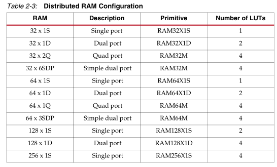
在IP核中,Block memory(distributed memory为CLB中的资源):

通常选用Native,而不用AXI接口:
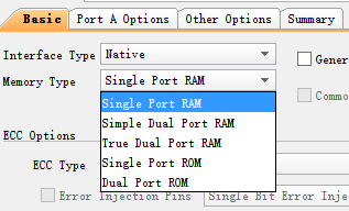
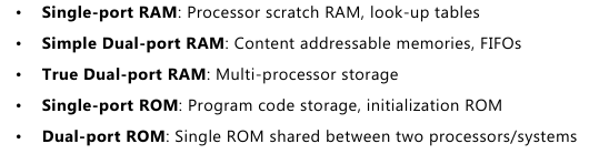
Block RAM可配置单端口RAM、伪双端口RAM、双端口RAM、单端口ROM、双端口ROM、FIFO。
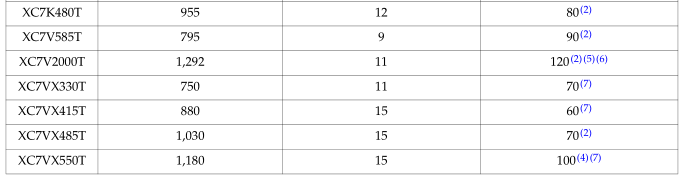
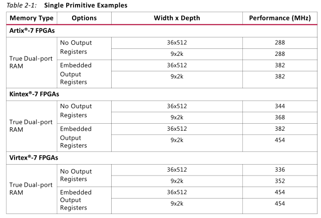
各个模式调用时可承受的最高频率,参考pg058.pdf:
二、主要功能
学习资源: http://www.asic-world.com/examples/verilog/memories.html

A-RAM/ROM
主要功能:
每一个Block RAM都可配置为1个36Kb的BRAM或1个36Kb的FIFO;同时也可以将其配置为2个单独的18Kb的BRAM或1个18KbBRAM + 1个18Kb的BRAM。
为什么是18k而不是16k(2的整次幂)?因为每8bit一个校验位。2*8 + 2 =18bit。
结论:无论是单端口RAM、伪双端口RAM还是双端口RAM,他们都只有一块Memory。
Single-port RAM:
同步示例:
module ram_sp_sr_sw (

clk         , // Clock Input

address     , // Address Input

data        , // Data bi-directional

cs          , // Chip Select

we          , // Write Enable/Read Enable

oe            // Output Enable

);

parameter DATA_WIDTH = 8 ;

parameter ADDR_WIDTH = 8 ;

parameter RAM_DEPTH = 1 << ADDR_WIDTH;

//--------------Input Ports-----------------------

input                  clk         ;

input [ADDR_WIDTH-1:0] address     ;

input                  cs          ;

input                  we          ;

input                  oe          ;

//--------------Inout Ports-----------------------

inout [DATA_WIDTH-1:0]  data       ;

//--------------Internal variables----------------

reg [DATA_WIDTH-1:0] data_out ;

reg [DATA_WIDTH-1:0] mem [0:RAM_DEPTH-1];

reg                  oe_r;

//--------------Code Starts Here------------------

// Tri-State Buffer control

// output : When we = 0, oe = 1, cs = 1

assign data = (cs && oe && !we) ? data_out : 8'bz;

// Memory Write Block

// Write Operation : When we = 1, cs = 1

always @ (posedge clk)

begin : MEM_WRITE

   if ( cs && we ) begin

       mem[address] = data;

   end

end

// Memory Read Block

// Read Operation : When we = 0, oe = 1, cs = 1

always @ (posedge clk)

begin : MEM_READ

  if (cs && !we && oe) begin

    data_out = mem[address];

    oe_r = 1;

  end else begin

    oe_r = 0;

  end

end

endmodule // End of Module ram_sp_sr_sw
异步(异步读、同步写)示例:
module ram_sp_ar_sw (

clk         , // Clock Input

address     , // Address Input

data        , // Data bi-directional

cs          , // Chip Select

we          , // Write Enable/Read Enable

oe            // Output Enable

);

parameter DATA_WIDTH = 8 ;

parameter ADDR_WIDTH = 8 ;

parameter RAM_DEPTH = 1 << ADDR_WIDTH;

//--------------Input Ports-----------------------

input                                     clk          ;

input [ADDR_WIDTH-1:0] address ;

input                                     cs           ;

input                                     we          ;

input                                     oe           ;

//--------------Inout Ports-----------------------

inout [DATA_WIDTH-1:0]  data       ;

//--------------Internal variables----------------

reg [DATA_WIDTH-1:0]   data_out ;

reg [DATA_WIDTH-1:0] mem [0:RAM_DEPTH-1];

//--------------Code Starts Here------------------

// Tri-State Buffer control

// output : When we = 0, oe = 1, cs = 1

assign data = (cs && oe && !we) ? data_out : 8'bz;

// Memory Write Block

// Write Operation : When we = 1, cs = 1

always @ (posedge clk)

begin : MEM_WRITE

   if ( cs && we ) begin

       mem[address] = data;

   end

end

// Memory Read Block

// Read Operation : When we = 0, oe = 1, cs = 1

always @ (address or cs or we or oe)

begin : MEM_READ

    if (cs && !we && oe) begin

         data_out = mem[address];

    end

end

endmodule // End of Module ram_sp_ar_sw
对应电路:
可以看出2^8 = 256由4个64拼接拼接而成:
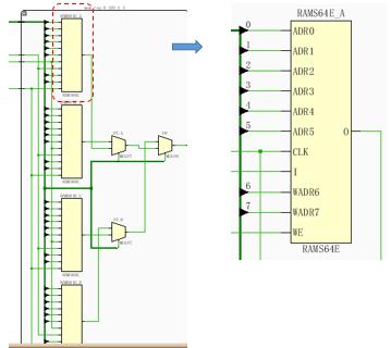
这里其实调用的是CLB中SliceM下的Distributed RAM资源:
B-FIFO
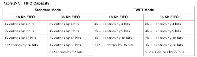
FIFO的能力:
FIFO的IP核使用,具体可参考:pg057.pdf。
FIFO可调用shift reg、distributed RAM、Block RAM、BulitIn FIFO,关于使用,xilinx论坛有相关说法:
Q:
From PG057 (Fifo generator) I understand FIFO's can be implemented in 4 ways, using :
- block RAM
- distributed RAM
- shift register
- built-in FIFO (using FIFO18 / FIFO36)
is there any simple document / app note / overview describing on what basis you typically decide between the 4 implementations. What are the main tradeoffs, advantages, ... of each underlying memory type used?
I can imagine a few, but not sure if these are correct and complete :
- block RAM is interesting for large, deep fifo's
- distributed RAM is interesting for smaller fifo's
- shift register is interesting for smaller fifo's, with short word width
- built-in FIFO allow for the fastest fifo's
but that's just intuition ... so any corrections or further insights are welcome here!
A:
Its based your application , requirement and available resources in your target FPGA. The most of the points you mention correct. I would recommend you to refer target FPGA resource guide LUTs have lowest access time, FIFO18/FIFO36 good timing performance but require effort in design migration, BRAM very good for scalable memory requirement . You can also check about URAM/ultraram available in ultrascale devices
三、IP核调用
A-simple dual RAM
参考IP_bram笔记。
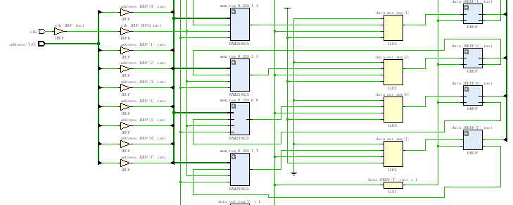
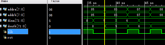
这里涉及到位宽的计算,以6通道,160MHz采样率,12bit有效位AD举例,现在需要转化为:240MHz的FPGA工作时钟。
12bit*6*160/240 = 48bit
位宽由12*6 = 72bit转化为48bit,:
- Port-A为写数据,width:位宽12*6 = 72bit,depth = 160
- Port-B为读数据,width:48bit,depth = 240
但Port-B的width只能是:72bit/(2^n),n = 0, ±1, ±2, ...,因此通常都是二次转化:
Step1:72*160 = 48*240 < x * 240,x = 72*2^n >48,此处n = 0;x工作在240MHz。
Step2:x * M = 48 * N,M、N都是整数。M = 1,N = 2,完成转化。
.png)
勾选primitive output register:
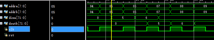
可见该选项延迟了1拍。
B-FIFO
主要参考:

关于IP核参数设置,可参考FIFO generator笔记。
与BRAM同样的例子,很多时候数据时钟域转换用dual-port RAM而不用FIFO,说是前者含地址,存在时延变量取数方便,但改为FIFO实现其实也可以,后者含有计数功能,同样可以进行定位。
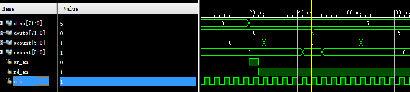
从读使能给出,到数据输出,经过6个周期,计算:
基础003_V7-Memory Resources的更多相关文章
- Understanding Virtual Memory
Understanding Virtual Memory by Norm Murray and Neil Horman Introduction Definitions The Life of a P ...
- DTrace to Troubleshoot Java Native Memory Problems
How to Use DTrace to Troubleshoot Java Native Memory Problems on Oracle Solaris 11 Hands-On Labs of ...
- Spring Boot Memory Performance
The Performance Zone is brought to you in partnership with New Relic. Quickly learn how to use Docke ...
- 再谈.net的堆和栈---.NET Memory Management Basics
.NET Memory Management Basics .NET memory management is designed so that the programmer is freed fro ...
- Allowing GPU memory growth
By default, TensorFlow maps nearly all of the GPU memory of all GPUs (subject to CUDA_VISIBLE_DEVICE ...
- CUDA ---- Memory Model
Memory kernel性能高低是不能单纯的从warp的执行上来解释的.比如之前博文涉及到的,将block的维度设置为warp大小的一半会导致load efficiency降低,这个问题无法用war ...
- Memory Leak Detection in C++
原文链接:http://www.linuxjournal.com/article/6556?page=0,0 An earlier article [“Memory Leak Detection in ...
- System and method for parallel execution of memory transactions using multiple memory models, including SSO, TSO, PSO and RMO
A data processor supports the use of multiple memory models by computer programs. At a device extern ...
- Move resources allocated using unmanaged interface to managed devm interface
转载:http://blog.csdn.net/swingboard/article/details/27207497 So today let’s talk about devm functio ...
- Find out when memory leaks are a concern and how to prevent them
Handling memory leaks in Java programs Find out when memory leaks are a concern and how to prevent t ...
随机推荐
- eclipse 远程调试程序
最近遇到一个非常恶心的问题,本地调试没有问题,到了线上就复发,逼于无奈只能使用eclipse远程调试,下面把步骤记录一下: 1.修改服务器的启动脚本,添加如下内容: export JPDA_ADDRE ...
- python 3使用binascii方法的报错解决
环境是python 3 问题: 使用binascii方法一直出现报错TypeError: a bytes-like object is required, not 'str' #coding: utf ...
- JavaBean与XML转换——XStream使用笔记
转载请注明原文地址:http://www.cnblogs.com/ygj0930/p/6648131.html 一:View层与Control层的数据交互 做过Web项目的人都知道,当对一个requ ...
- Java中equals()和hashCode()的关系以及重写equals()和hashCode()的重要性
转载请注明原文地址:http://www.cnblogs.com/ygj0930/p/6580647.html 一:关系 如果两个对象相等(equal),它们的hashcode一定相同: 如果两个对 ...
- maximum-subarray 序列最大连续和 贪心
Find the contiguous subarray within an array (containing at least one number) which has the largest ...
- 【AIX】在命令前显示完整路径
登录到AIX系统,发现在#前没有目录展示,这样我们在查看当前目前时很不方便,需要借助命令PWD才可以实现 解决方案: 在.profile文件中添加命令:export PS1="[LONGNA ...
- Linux人工清理内存cache
内存缓存的出现是解决,设备之间的读写速度的差异! 00.linux缓存解释 /proc/sys/vm/drop_caches (since Linux 2.6.16)Writing to this ...
- Linux下Shell元字符的释义
Linux下shell的巧妙应用,对系统的运维很有四两拨千斤的功效! Shell元字符 注意: () 在当前shell的子shell进程运行命令 {}在当前shell进程运行命令
- Spring Cloud开发实践 - 04 - Docker部署
Docker的安装和命令可以参考 https://www.cnblogs.com/milton/p/9866963.html . 资源规划 这一步要区分传统资源和Docker资源, 为后面的细节定好基 ...
- windows下Oracle Tuxedo编译应用前需要配置的相关环境变量
rem (c) BEA Systems, Inc. All Rights Reserved. rem Copyright (c) BEA Systems, Inc. rem All Rights Re ...