
STA之OCV
Timing sign-off Corner = library PVT +RC Corner + OCV
针对每个工艺结点,foundry都会给出一张类似的timing sign-off表格,定义了所有需要做timing sign-off的corner(实际需要sign-off的corner还需要乘以工作模式,对于STA,不同的工作模式,用不同的SDC文件予以区别)

uncertainty=clock jitter + Xps setup/hold margin + DPT,其中clock jitter由用户根据所用PLL的精度来确定;Xps由foundry提供,如:30ps for setup, 40ps for hold; DPT一项表示需要加的额外margin用于cover mask misalignment引起的偏差,该值亦由foundary提供,比如5ps for setup, 3ps for hold。
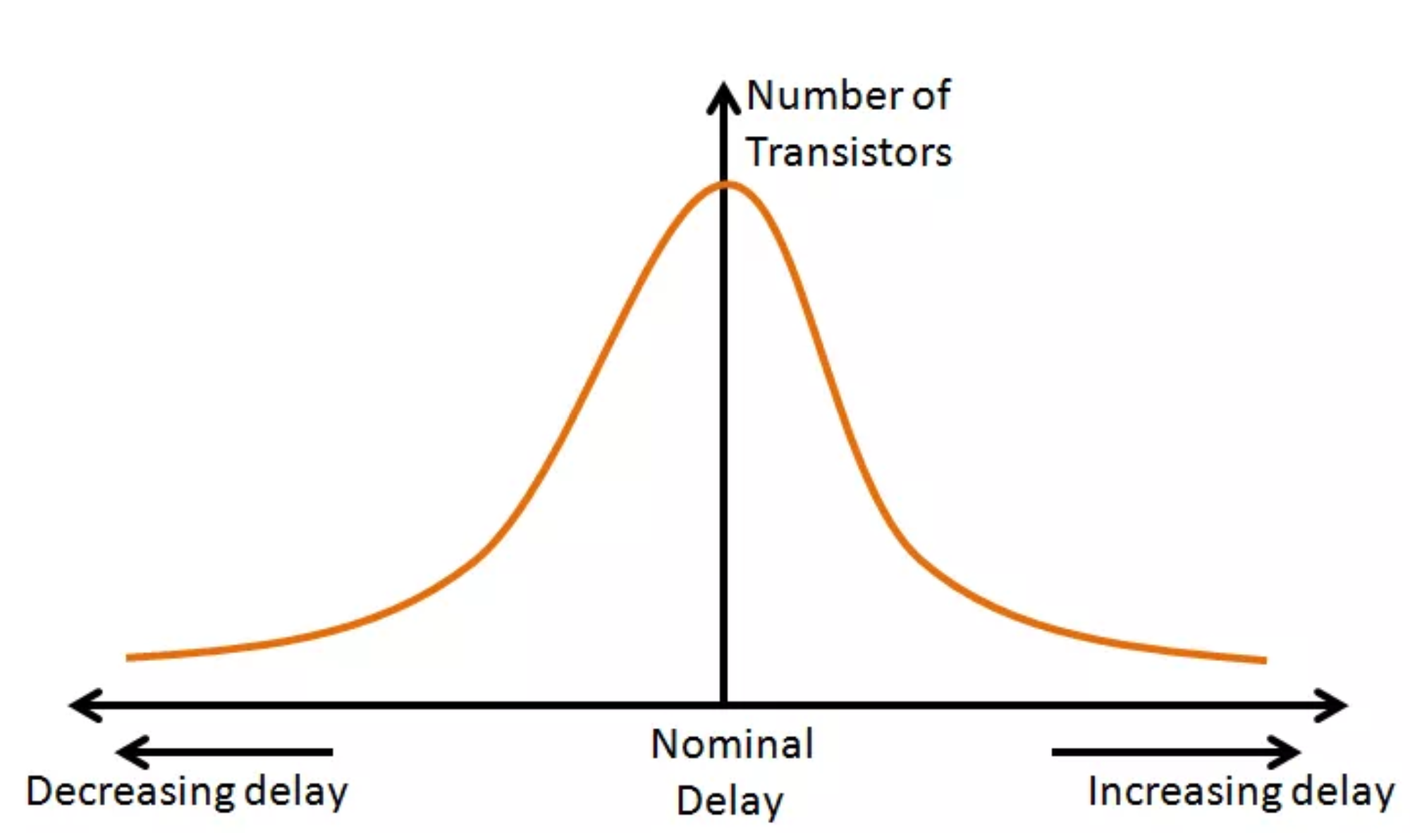
世界上没有两片相同的叶子,半导体世界里没有两只相同的管子。library中的cell delay是在某个固定的PVT(operating condition)下仿真得出的,也就是下图中的Nominal delay,而实际上在芯片内部由于工艺偏差、电压降、温度变化,cell的delay并不是一个固定值,而是一个随机值,遵循高斯分布或门特卡洛分布。
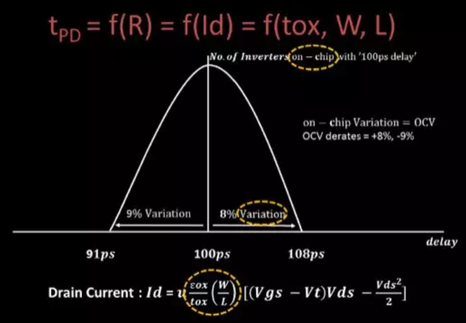
在STA中用OCV来模拟这一『特征』,OCV全称on chip variation,用于描述不同管子间由于工艺偏差、电压降、温度变化引起的delay变化,也用于描述工艺偏差引起的net厚度宽度的变化从而导致net的电容电阻变化。
PVT跟OCV都是用于描述Process、Voltage、Temperature对timing的影响,两者有何区别?
PVT:主要取决于外部因素,在某一固定的工艺点、芯片的工作电压、周围环境温度对芯片性能的影响。更直白的理解:同一颗芯片在不同工作电压、环境温度下的性能表现。
OCV:用于模拟芯片内部不同管子由于工艺偏差、电压降、温度变化引起的性能变化,这种变化更宏观的表现是:不同芯片在相同PVT下的性能表现不同。
在timing sign-off时,为什么要在Nominal delay上加OCV?
因为Nominal delay是在固定PVT下仿真得出的delay,而实际上由于OCV的影响,管子的delay是呈高斯分布或门特卡洛分布,要想保证yield,就必须在timing sign-off时将OCV考虑在内,以保证大部分管子都可以满足时序要求。对每一代工艺,foundry都会做大量测试,针对每个corner找到一组适合的OCV值,这组值可以保证足够高的yield,而如果进一步加紧这个值,并不会更有效的提高yield。在SOCV/POCV里的多少sigma(如:3-sigma)的选取也是出于相同的考虑
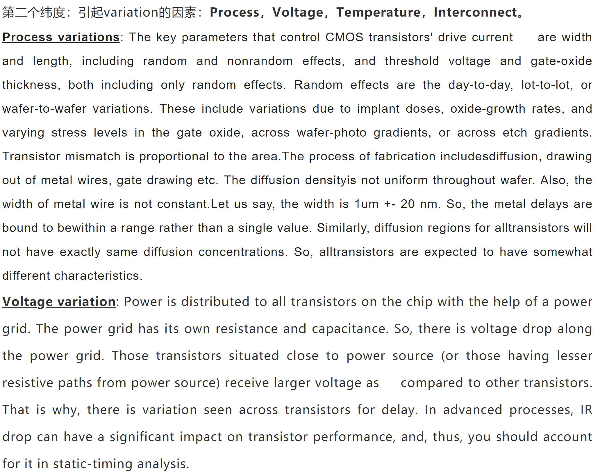
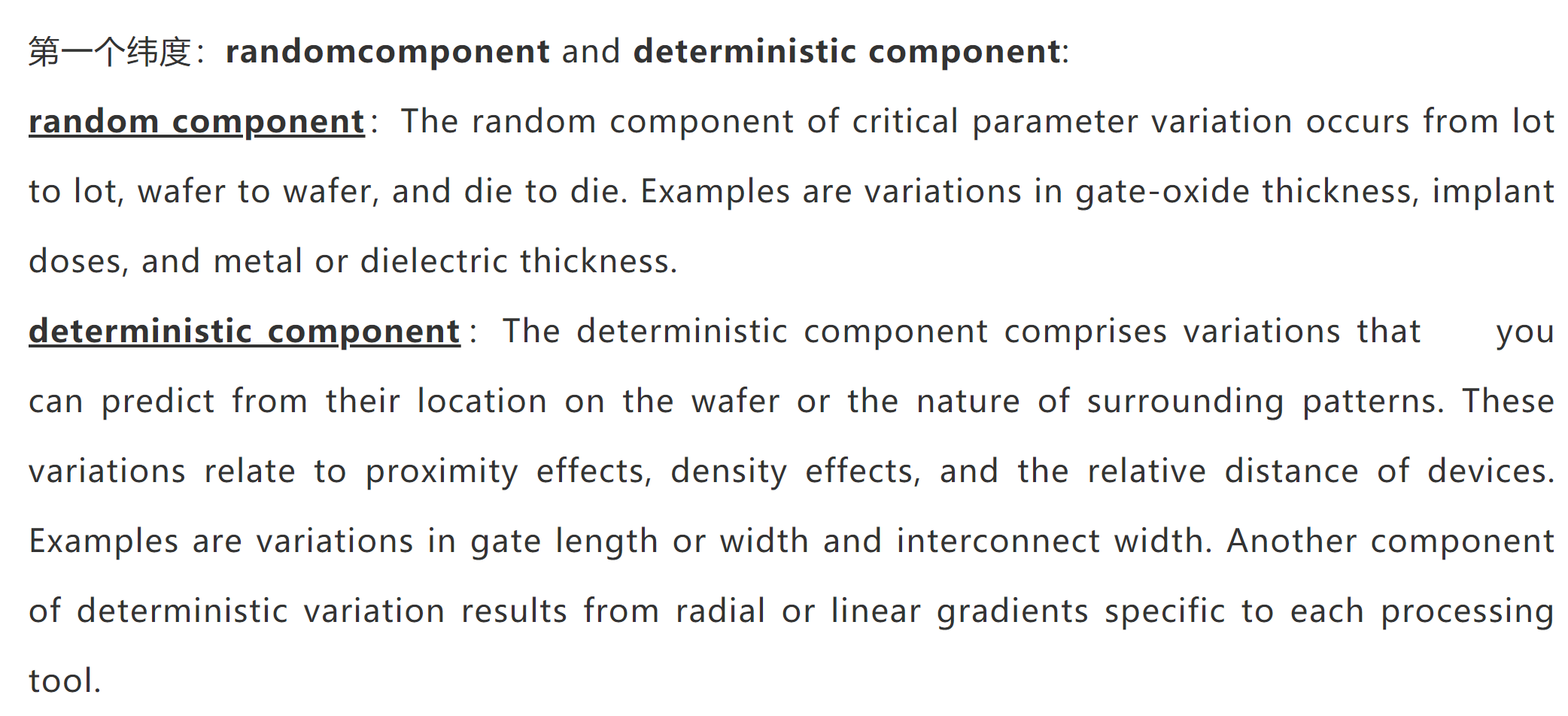
Interconnect variation: Another area of on-chip variation is in interconnect height and width, resulting in variation in both resistance and capacitance. Because the delay from interconnect is becoming more dominant as geometries shrink, you should pay attention to accurate modeling of interconnect variations. Two potential sources of this variation are the CMP (chemical-mechanical-planarization) process and the proximity effects in the photolithography and etch processes. Variation in the CMP process results from the difference in hardness between the interconnect material and the dielectric. Ideally, after the designer has etched trenches into the dielectric below an interconnect layer and copper on the wafer, the CMP process removes the unwanted copper, leaving only lines and vias. The copper line is softer than the dielectric material, resulting in "dishing" and erosion, which cause uneven removal of the copper and dielectric. Dishing is a function of line width and density, and erosion is a function of line space and density. Another source of variation in thickness due to CMP is a morerandom variation resulting in a gradient across the wafer. You can see thisgradient in die-to-die variations and even across-die variations for large die.You would ideally model this random, nondeterministic variation statistically.However, if you can obtain process data to model this variation, then you canmodel it deterministically as a function of position on the wafer. In thisscenario, you give an adder or subtracter, depending on the x,y position on thedie, to the RC value. Etch-proximity effects appear as "microloading," whichmeans that the etch process overetches isolated lines. A dual-damascenestructure uses only a single metal-deposition step to simultaneously form themain metal lines and the metal in the vias. That is, the formation of both thetrenches and the vias occurs in one dielectric layer. Overetching results in awider trench and, hence, a wider metal line. Photolithographic effects also cause problems. Diffraction andlocal scattering in photolithography may overexpose densely spaced lines andunderexpose isolated lines. Tiling and metal slotting reduce the variation infeature density and mitigate these effects. Tiling algorithms give differentresults, but a general rule states that a less dense gradient yields smallerline-width variations on the die. Tiling does have its drawbacks, however. Asone of the last integration steps in an SOC-design flow, tiling involvescalculations that the extractor performs using density parameters. Thesecalculations can result in different RC values before and after tiling. Tilingcan also result in small additional delay effects on timing. The final designmay not meet the desired target frequency once you account for tiling. Whetherit does depends largely on the design and the methods you use to meet thetiling requirements.
方法学上概念清晰了之后,EDA工具端的操作就十分简单了,在EDA工具中如何设置OCV?每家工具都有各自不同的命令/变量控制,跟OCV相关的大致可分为四部分,此处以Tempus的命令为例:
全局控制:set_analysis_mode -analysisType onChipVariation
设置OCV:set_timing_derate -cell_delay/net_delay/cell_check -late/early -data/clock (1-d%);其中d%是foundry在sign-off表格中给出的OCV值
Report OCV: report_statistical_timing_derate_factors
Debug timing时在timing report中将derate列显示出来:set_global report_timing_format {instance arc delay slew arrival user_derate}
由于工艺的进步,flat OCV在先进工艺如16,7中已经逐步被AOCV, SOCV/POCV取代,以剔除悲观度。
STA之OCV的更多相关文章
- STA之PVT
在STA星球,用library PVT.RC corner跟OCV来模拟这些不可控的随机因素.在每个工艺结点,通过大量的建模跟实测,针对每个具体的工艺,foundary厂都会提供一张推荐的timing ...
- 论STA | 工艺、工具、分析的本与末
人类从漫长的蒙昧中觉醒之后,不再依靠着奇装异服的巫师通灵来指导生活,巫师进化成了科学家,他们试图对周遭的一切进行概括.分类.抽象,于是有了化学.物理.数学等基科.比如一粒沙,它的化学组成是什么,物理特 ...
- 论STA | SOCV / POCV 之 variation (2)
芯片制造涉及到许多复杂重复的过程,如:光刻.蚀刻.离子注入.扩散.退火.而且都是原子级操作,尽管控制非常严格,但偏差不可避免. 工艺偏差会导致芯片物理参数偏差,如:线宽.沟道掺杂浓度.线厚.临界尺寸. ...
- STA之AOCV
为什么要引入AOCV 为了精确性,为了剔除悲观度.用set_timing_derate来设置OCV,对于一个固定的corner,只能对data/clock, cell/net, late/early分 ...
- 选择目录,选择文件夹的COM组件问题。在可以调用 OLE 之前,必须将当前线程设置为单线程单元(STA)模式。请确保您的 Main 函数带有 STAThreadAttribute 标记。 只有将调试器附加到该进程才会引发此异常。
异常: 在可以调用 OLE 之前,必须将当前线程设置为单线程单元(STA)模式.请确保您的 Main 函数带有 STAThreadAttribute 标记. 只有将调试器附加到该进程才会引发此异常. ...
- 【转】使用SQL Tuning Advisor STA优化SQL
SQL优化器(SQL Tuning Advisor STA)是Oracle10g中推出的帮助DBA优化工具,它的特点是简单.智能,DBA值需要调用函数就可以给出一个性能很差的语句的优化结果.下面介绍一 ...
- 如何用 SQL Tuning Advisor (STA) 优化SQL语句
在Oracle10g之前,优化SQL是个比较费力的技术活,不停的分析执行计划,加hint,分析统计信息等等.在10g中,Oracle推出了自己的SQL优化辅助工具: SQL优化器(SQL Tuning ...
- [BZOJ1131][POI2008] Sta 树的深度
Description 给出一个N个点的树,找出一个点来,以这个点为根的树时,所有点的深度之和最大 Input 给出一个数字N,代表有N个点.N<=1000000 下面N-1条边. Output ...
- 在可以调用 OLE 之前,必须将当前线程设置为单线程单元(STA)模式
在可以调用 OLE 之前,必须将当前线程设置为单线程单元(STA)模式 转载自:http://blog.163.com/smhily_min/blog/static/75206226201092011 ...
随机推荐
- java通过浏览器请求头(User-Agent)获取访问者设备信息以及系统版本
个人博客 地址:http://www.wenhaofan.com/article/20181125220342 在开发AutuBlog项目时需要做后台的登录记录,想起浏览器的User-Agent,于是 ...
- 移动端调试神器vConsole
vConsole.js 其实就是重写console方法,实现了类似于微信小程序的移动端调试效果 在普通html文件里使用 <script src="https://cdn.bootcs ...
- mui H5+ 调取 相册 拍照 功能 上传图片 + 裁剪功能
H5+ 相册拍照图片上传 点击用户头像后,弹出actionSheet,选择从相册或是拍照:选取照片后调用上传方法: 上传图片后调用PhotoClip.js 插件进行裁剪 具体流程 弹出actionS ...
- (原创)SpringBoot入门
本文章是SpringBoot入门的介绍在这里 我会尽量写一些细节性的东西,我用的是IDEA2016 Tomcat7 JDK1.8 Maven3.3.9 IDEA Tomcat JDK Maven ...
- importing-cleaning-data-in-r-case-studies
目录 importing-cleaning-data-in-r-case-studies 导入数据 查看数据结构 下面的一些都是查数据结构的 separate 拆分单元格 读取指定位置的数据 stri ...
- Xshell5配置ssh免密码登录-公钥与私钥登录linux服务器(xshell如何登陆上阿里云服务器)
原文地址:https://blog.csdn.net/longgeaisisi/article/details/78680180 ssh登录提供两种认证方式:口令(密码)认证方式和密钥认证方式.其中口 ...
- 【18】 递归 X的N次幂
题目(我没想到这也能出成题目--) 实现函数double Power(double base, int exponent),求base的exponent次方.不得使用库函数,同时不需要考虑大数问题. ...
- vscode+vue 一些基本操作
1.安装好 vscode 和 node.js 安装node.js是为了用npm(管理项目依赖) 2.调出终端 crtl +~ , 3.终端全局安装 vue-cli 安装整个脚手架,能快速给我们构建v ...
- RGBA alpha 透明度混合算法
RGBA alpha 透明度混合算法 .分类: 图像处理 Ps技术 2011-05-25 09:11 1112人阅读 评论(0) 收藏 举报 Alpha 透明度混合算法,网上收集整理,分成以下三种: ...
- C++-对象指针的滥用
C++ 中经常出现使用对象指针,而不是直接使用对象本身的代码,比如下面这个例子: Object *myObject = new Object; 而不是使用: myObject.testFunc(); ...