Voltage Translation for Analog to Digital Interface ADC
Voltage Translation for Analog to Digital Interface
孕龙逻辑分析仪 ZeroPlus Logic Analyzer
How to modify analog output range of Arduino Due
In today's microcontroller market, most of the Analog to Digital converters
are only able to accept voltages from the Vcc of the device to ground.
But what if you want to measure a bipolar signal?
This short tutorial plans to show you a simple but effective method
to interface a bipolar voltage to any single polarity input.
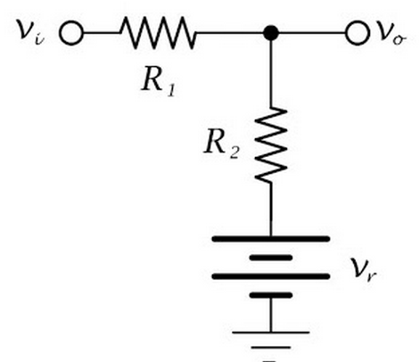
On the left is the ideal basic circuit for interfacing.
vi is the input voltage, vo is the voltage sent to the ADC,
vr is a reference voltage used for setting the center or zero input voltage,
and R1 and R2 are used for input scaling and current limiting
to bring the input voltage into the range of the ADC.
- Input impedance of at least 1Mohm.
- vin = +/- 12V
- vo = 0-5V
So when vin = 12v, vo = 5v
vin = -12v, vo = 0v
vin = 0v, vo = 2.5v
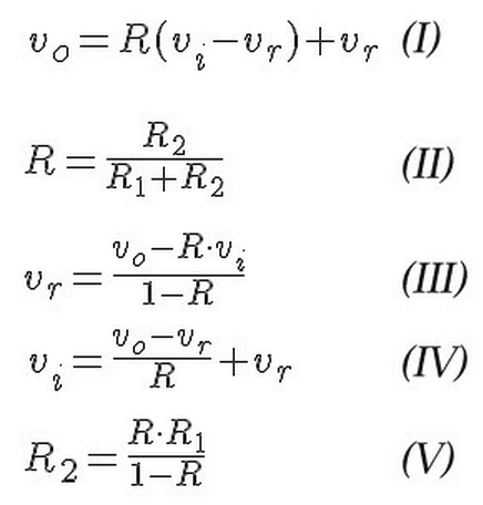
To begin, I need to calculate the value of R
R2 = (R * R1)/(1-R) = (.2083 * 1M)/(1-.2083) = 208,300/.7917 = 263,104 ohms.
Next I need to calculate the value of vr.
Using the case of vin = 12, vo = 5, and using formula III:
vr = (vo - R * vi)/(1 - R) = (5 - .2083 * 12)/(1 - .2083) = 2.5004/.7917 = 3.158v
I now have the 3 values required for my design.
R1 = 1M
R2 = 263,104
vr = 3.158v
vo (vin=+12) = R(vi - vr) + vr = .2083(12 - 3.158) + 3.158 = 5.000
vo (vin= 0) = .2083(0 - 3.158) + 3.158 = 2.500
vo (vin=-12) = .2083(-12 - 3.158) + 3.158 = 0
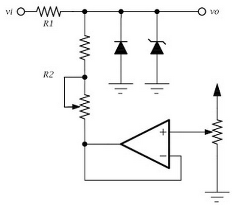
To the left is a practical circuit to interface to an ADC. The features are:
- A diode and zener diode used to protect the ADC input from overvoltage.
- R2 is composed of a fixed value, and a trim pot to dial in the correct value.
- A trim pot connected to the non inverting input of an op amp in a voltage follower configuration for setting vr.
Now I have a working circuit, but the last thing to calculate is the maximum and minimum input voltages.
vi = ((vo - vr)/R) + vr = ((5.1 - 3.158)/.2083) + 3.158 = 12.481v
The minimum input voltage will occur when the diode is forward biased.
vi = ((-0.7 - 3.158)/.2083) + 3.158 = -15.363v
Effective input impedance can be calculated as follows:
zin = vin(R1 + R2)/(vin - vr)
This is a varying quantity depending on vin.
Voltage Translation for Analog to Digital Interface ADC的更多相关文章
- Fully Digital Implemented Delta-Sigma Analog to Digital Converter
http://www.design-reuse.com/articles/14886/fully-digital-implemented-delta-sigma-analog-to-digital-c ...
- Analog/digital converter (ADC)
1.ADC1 and ADC2 are 10-bit successive approximation Anolog to Digital Converters. 所谓successive appro ...
- STM8S——Analog/digital converter (ADC)
1.ADC1 and ADC2 are 10-bit successive approximation Anolog to Digital Converters. 所谓successive appro ...
- DG449 High Voltage Single SPDT Analog Switch in SOT23-8
DESCRIPTION The DG449 is a dual supply single-pole/double-throw (SPDT) switches. On resistance is 38 ...
- How to modify analog output range of Arduino Due
Voltage Translation for Analog to Digital Interface ADC How to modify analog output range of Arduino ...
- 孕龙逻辑分析仪 ZeroPlus Logic Analyzer
Voltage Translation for Analog to Digital Interface ADC http://openschemes.com/2010/03/23/zeroplus-l ...
- quick start guide for XMEGA ADC
This is the quick start guide for the Analog to Digital Converter (ADC), with step-by-step instructi ...
- BOOST Converter Analog/Digital Adjusted Output Voltage TPS61045 MAX1932
DIGITALLY ADJUSTABLE BOOST CONVERTER The TPS61045 is a high frequency boost converter with digitally ...
- Digital Adjustment of DC-DC Converter Output Voltage in Portable Applications
http://pdfserv.maximintegrated.com/en/an/AN818.pdf http://www.maximintegrated.com/app-notes/index.mv ...
随机推荐
- App调试的几个命令实践【转】
在Android的应用开发中,我们会用到各种代码调试:其实在Android的开发之后,我们可能会碰到一些随机的问题,如cpu过高,内存泄露等,我们无法简单的进行代码调试,我们需要一个系统日志等等,下面 ...
- SQL Server 触发器demo
GO /****** Object: Trigger [dbo].[tri_device] Script Date: 2018/6/11 10:56:08 ******/ SET ANSI_NUL ...
- Linux下进程/程序网络带宽占用情况查看工具 -- NetHogs
http://www.vpser.net/manage/nethogs.html 来自. 最后略有修改 之前VPS侦探曾经介绍过流量带宽相关的工具如:iftop.vnstat,这几个都是统计和监 ...
- python通过Cookie跳过登录验证码
1.通过浏览器获取登录cookie,找到重要的两个参数“BAIDUID”和“BDUSS”: 2.编写Selenium自动化测试脚本,跳过登录. from selenium import webdriv ...
- log4j2 使用详解
转载自 Blog of 天外的星星: http://www.cnblogs.com/leo-lsw/p/log4j2tutorial.html Log4j 2的好处就不和大家说了,如果你搜了2,说明你 ...
- ambari下的flume和kafka整合
1.配置flume #扫描指定文件配置 agent.sources = s1 agent.channels = c1 agent.sinks = k1 agent.sources.s1.type=ex ...
- 将模型.pb文件在tensorboard中展示结构
本文介绍将训练好的model.pb文件在tensorboard中展示其网络结构. 1. 从pb文件中恢复计算图 import tensorflow as tf model = 'model.pb' # ...
- 自动化测试使用cookie跳过验证码
准备工具: fiddler Python+selenium 安装fidder fidder官方下载地址 fidder首次安装需要设置才能抓取https参考如下 fidder设置抓取https 开始 1 ...
- RabbitMQ(一):RabbitMQ 安装与配置(Mac)
一.rabbitmq 安装与配置 安装: brew install rabbitmq # 进入安装目录 cd /usr/local/Cellar/rabbitmq/3.7.12 # 启动 brew s ...
- Linux !的使用
转自:https://www.linuxidc.com/Linux/2015-05/117774.htm 一.history 78 cd /mnt/ 79 ls 80 cd / 81 history ...