Voltage Translation for Analog to Digital Interface ADC
Voltage Translation for Analog to Digital Interface
孕龙逻辑分析仪 ZeroPlus Logic Analyzer
How to modify analog output range of Arduino Due
In today's microcontroller market, most of the Analog to Digital converters
are only able to accept voltages from the Vcc of the device to ground.
But what if you want to measure a bipolar signal?
This short tutorial plans to show you a simple but effective method
to interface a bipolar voltage to any single polarity input.
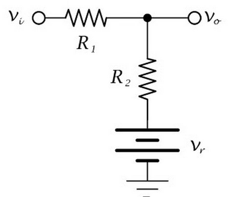
On the left is the ideal basic circuit for interfacing.
vi is the input voltage, vo is the voltage sent to the ADC,
vr is a reference voltage used for setting the center or zero input voltage,
and R1 and R2 are used for input scaling and current limiting
to bring the input voltage into the range of the ADC.
- Input impedance of at least 1Mohm.
- vin = +/- 12V
- vo = 0-5V
So when vin = 12v, vo = 5v
vin = -12v, vo = 0v
vin = 0v, vo = 2.5v
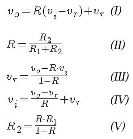
To begin, I need to calculate the value of R
R2 = (R * R1)/(1-R) = (.2083 * 1M)/(1-.2083) = 208,300/.7917 = 263,104 ohms.
Next I need to calculate the value of vr.
Using the case of vin = 12, vo = 5, and using formula III:
vr = (vo - R * vi)/(1 - R) = (5 - .2083 * 12)/(1 - .2083) = 2.5004/.7917 = 3.158v
I now have the 3 values required for my design.
R1 = 1M
R2 = 263,104
vr = 3.158v
vo (vin=+12) = R(vi - vr) + vr = .2083(12 - 3.158) + 3.158 = 5.000
vo (vin= 0) = .2083(0 - 3.158) + 3.158 = 2.500
vo (vin=-12) = .2083(-12 - 3.158) + 3.158 = 0
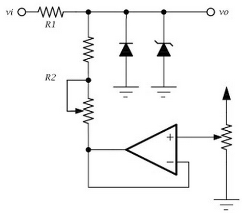
To the left is a practical circuit to interface to an ADC. The features are:
- A diode and zener diode used to protect the ADC input from overvoltage.
- R2 is composed of a fixed value, and a trim pot to dial in the correct value.
- A trim pot connected to the non inverting input of an op amp in a voltage follower configuration for setting vr.
Now I have a working circuit, but the last thing to calculate is the maximum and minimum input voltages.
vi = ((vo - vr)/R) + vr = ((5.1 - 3.158)/.2083) + 3.158 = 12.481v
The minimum input voltage will occur when the diode is forward biased.
vi = ((-0.7 - 3.158)/.2083) + 3.158 = -15.363v
Effective input impedance can be calculated as follows:
zin = vin(R1 + R2)/(vin - vr)
This is a varying quantity depending on vin.
Voltage Translation for Analog to Digital Interface ADC的更多相关文章
- Fully Digital Implemented Delta-Sigma Analog to Digital Converter
http://www.design-reuse.com/articles/14886/fully-digital-implemented-delta-sigma-analog-to-digital-c ...
- Analog/digital converter (ADC)
1.ADC1 and ADC2 are 10-bit successive approximation Anolog to Digital Converters. 所谓successive appro ...
- STM8S——Analog/digital converter (ADC)
1.ADC1 and ADC2 are 10-bit successive approximation Anolog to Digital Converters. 所谓successive appro ...
- DG449 High Voltage Single SPDT Analog Switch in SOT23-8
DESCRIPTION The DG449 is a dual supply single-pole/double-throw (SPDT) switches. On resistance is 38 ...
- How to modify analog output range of Arduino Due
Voltage Translation for Analog to Digital Interface ADC How to modify analog output range of Arduino ...
- 孕龙逻辑分析仪 ZeroPlus Logic Analyzer
Voltage Translation for Analog to Digital Interface ADC http://openschemes.com/2010/03/23/zeroplus-l ...
- quick start guide for XMEGA ADC
This is the quick start guide for the Analog to Digital Converter (ADC), with step-by-step instructi ...
- BOOST Converter Analog/Digital Adjusted Output Voltage TPS61045 MAX1932
DIGITALLY ADJUSTABLE BOOST CONVERTER The TPS61045 is a high frequency boost converter with digitally ...
- Digital Adjustment of DC-DC Converter Output Voltage in Portable Applications
http://pdfserv.maximintegrated.com/en/an/AN818.pdf http://www.maximintegrated.com/app-notes/index.mv ...
随机推荐
- 通达OA在centos系统中快速部署文档(web和数据库)
通达OA2008从windows环境移植到linux中(centos5.5及以上版本) 如果安装好了,还是无法访问,则需要清空浏览器缓存即可 1.安装lamp环境,这里用的是xampp集成安装包xam ...
- 在Android开发中,定时执行任务的3种实现方法
在Android开发中,定时执行任务的3种实现方法: 一.采用Handler与线程的sleep(long)方法(不建议使用,Java的实现方式)二.采用Handler的postDelayed(Runn ...
- MyCP(课下作业,必做)
作业要求 编写MyCP.java 实现类似Linux下cp XXX1 XXX2的功能,要求MyCP支持两个参数: java MyCP -tx XXX1.txt XXX2.bin 用来把文本文件(内容为 ...
- SQL中的 if 结构和循环(while)结构
- WPF 绑定 验证
<TextBox Grid.Column="1" Margin="1" Text="{Binding Name, ValidatesOnExce ...
- 【Algorithm | 链表】单链表“环”、“环的起点”、“环的长度”问题
参考资料 • Floyd判圈算法 { 链接 } • 单链表“环”.“环的起点”.环的长度”问题 { 链接 } 链表环的问题 一.判断链表有换 使用两个指针slow和fast.两个指针开始时均在头节点处 ...
- poj 1256 按一定顺序输出全排列(next_permutation)
Sample Input 3aAbabcacbaSample Output AabAbaaAbabAbAabaAabcacbbacbcacabcbaaabcaacbabacabcaacabacbaba ...
- java快速排序引起的StackOverflowError异常
写在前面:这篇随笔主要记录一下递归调用引起的虚拟机栈溢出的情况以及通过参数配置了虚拟机栈大小来使递归调用可以顺利执行.并没有对涉及到的一些概念进行详细的解释(因为我自己目前对这些概念并不是特别清楚), ...
- Maven的下载,安装,配置,测试,初识以及Maven私服
:Maven目录分析 bin:含有mvn运行的脚本 boot:含有plexus-classworlds类加载器框架 conf:含有settings.xml配置文件 lib:含有Maven运行时所需要的 ...
- (第1篇)什么是hadoop大数据?我又为什么要写这篇文章?
摘要: hadoop是什么?hadoop是如何发展起来的?怎样才能正确安装hadoop环境? 这些天,有很多人咨询我大数据相关的一些信息,觉得大数据再未来会是一个朝阳行业,希望能尽早学会.入行,借这个 ...