
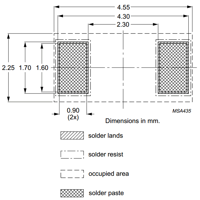
SMT Surface Mount Technology footprint references
http://en.wikipedia.org/wiki/Surface-mount_technology
Surface-mount technology (SMT) is a method for producing electronic circuits in which the components are mounted or placed directly onto the surface of printed circuit boards (PCBs).
An electronic device so made is called a surface-mount device (SMD).
In the industry it has largely replaced the through-hole technology construction method of fitting components with wire leads into holes in the circuit board.
Both technologies can be used on the same board for components not suited to surface mounting such as large transformers and heat-sinked power semiconductors.
An SMT component is usually smaller than its through-hole counterpart because it has either smaller leads or no leads at all. It may have short pins or leads of various styles, flat contacts, a matrix of solder balls (BGAs), or terminations on the body of the component.
Because "surface-mount" refers to a methodology of manufacturing, there are different terms used when referring to the different aspect of the method, which distinguishes for example the components, technique and machines used in manufacturing. These terms are listed in the following table:
| SMp term | Expanded form |
|---|---|
| SMD | Surface-mount devices (active, passive and electromechanical components) |
| SMT | Surface-mount technology (assembling and mounting technology) |
| SMA | Surface-mount assembly (module assembled with SMT) |
| SMC | Surface-mount components (components for SMT) |
| SMP | Surface-mount packages (SMD case forms) |
| SME | Surface-mount equipment (SMT assembling machines) |
Surface-mount components are usually smaller than their counterparts with leads, and are designed to be handled by machines rather than by humans. The electronics industry has standardized package shapes and sizes (the leading standardisation body is JEDEC). These include:
The codes given in the chart below usually tell the length and width of the components in tenths of millimeters or hundredths of inches.
For example, a metric 2520 component is 2.5mm by 2.0mm which corresponds roughly to .10 inches by .08 inches (hence, imperial size is 1008).
Exceptions occur for imperial in the two smallest rectangular passive sizes. The metric codes still represent the dimensions in mm, even though the imperial size codes are no longer aligned.
Problematically, some manufacturers are developing metric components with dimensions of name is already being used for the 0.4 mm × 0.2 mm (0.016 in × 0.0079 in) package.
Example of component sizes, metric and imperial codes and comparison included
- Two-terminal packages
- Rectangular passive components (mostly resistors and capacitors):
- 01005 (0402 metric): 0.4 mm × 0.2 mm (0.016 in × 0.0079 in). Typical power rating for resistors = 0.031 watt[8]
- 0201 (0603 metric): 0.6 mm × 0.3 mm (0.024 in × 0.012 in). Typical power rating for resistors = 0.05 watt[8]
- 0402 (1005 metric): 1.0 mm × 0.5 mm (0.039 in × 0.020 in). Typical power rating for resistors = 0.1 [8]or 0.062 watt[9]
- 0603 (1608 metric): 1.6 mm × 0.8 mm (0.063 in × 0.031 in). Typical power rating for resistors = 0.1 watt[8]
- 0805 (2012 metric): 2.0 mm × 1.25 mm (0.079 in × 0.049 in). Typical power rating for resistors = 0.125 watt[8]
- 1008 (2520 metric): 2.5 mm × 2.0 mm (0.098 in × 0.079 in). Typical inductor and ferrite bead package[10]
- 1206 (3216 metric): 3.2 mm × 1.6 mm (0.13 in × 0.063 in). Typical power rating for resistors = 0.25 watt[8]
- 1210 (3225 metric): 3.2 mm × 2.5 mm (0.13 in × 0.098 in). Typical power rating for resistors = 0.5 watt[8]
- 1806 (4516 metric): 4.5 mm × 1.6 mm (0.18 in × 0.063 in)[11]
- 1812 (4532 metric): 4.5 mm × 3.2 mm (0.18 in × 0.13 in). Typical power rating for resistors = 0.75 watt[8]
- 2010 (5025 metric): 5.0 mm × 2.5 mm (0.20 in × 0.098 in). Typical power rating for resistors = 0.75 watt[8]
- 2512 (6332 metric): 6.4 mm × 3.2 mm (0.25 in × 0.13 in). Typical power rating for resistors = 1 watt[8]
- 2920: 7.4 mm × 5.1 mm (0.29 in × 0.20 in)[12]

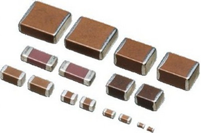

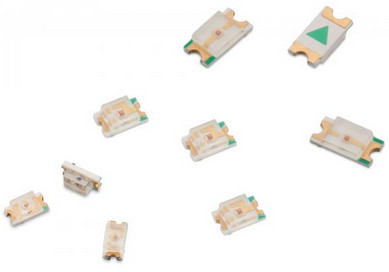
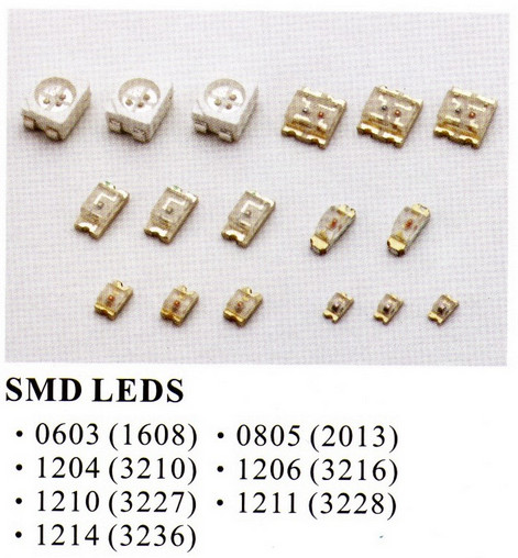
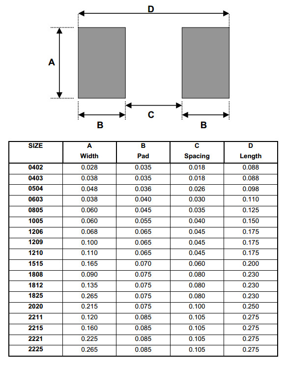

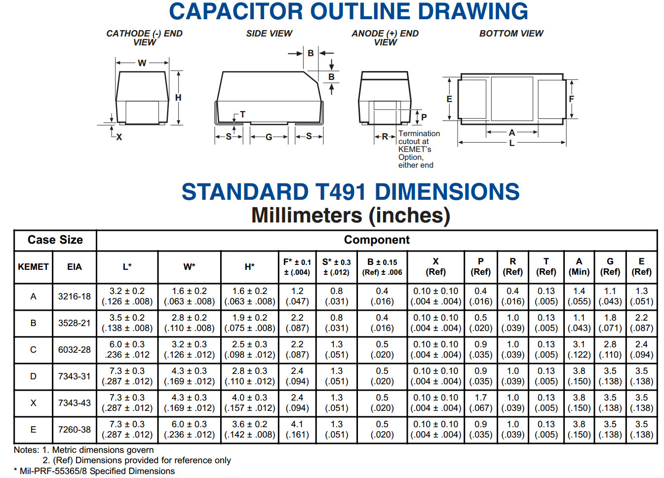
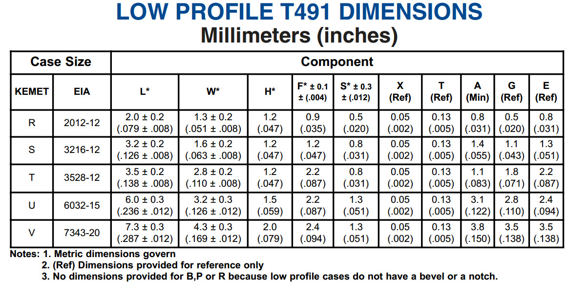
- Tantalum capacitors length (typ.) x width (typ.) x height (max.):[13][14]
- EIA 2012-12 (Kemet R, AVX R): 2.0 mm × 1.3 mm × 1.2 mm
- EIA 3216-10 (Kemet I, AVX K): 3.2 mm × 1.6 mm × 1.0 mm
- EIA 3216-12 (Kemet S, AVX S): 3.2 mm × 1.6 mm × 1.2 mm
- EIA 3216-18 (Kemet A, AVX A): 3.2 mm × 1.6 mm × 1.8 mm
- EIA 3528-12 (Kemet T, AVX T): 3.5 mm × 2.8 mm × 1.2 mm
- EIA 3528-21 (Kemet B, AVX B): 3.5 mm × 2.8 mm × 2.1 mm
- EIA 6032-15 (Kemet U, AVX W): 6.0 mm × 3.2 mm × 1.5 mm
- EIA 6032-28 (Kemet C, AVX C): 6.0 mm × 3.2 mm × 2.8 mm
- EIA 7260-38 (Kemet E, AVX V): 7.3 mm × 6.0 mm × 3.8 mm
- EIA 7343-20 (Kemet V, AVX Y): 7.3 mm × 4.3 mm × 2.0 mm
- EIA 7343-31 (Kemet D, AVX D): 7.3 mm × 4.3 mm × 3.1 mm
- EIA 7343-43 (Kemet X, AVX E): 7.3 mm × 4.3 mm × 4.3 mm
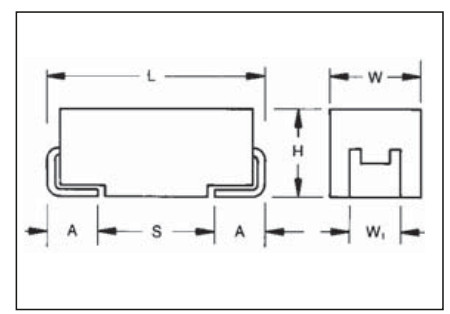
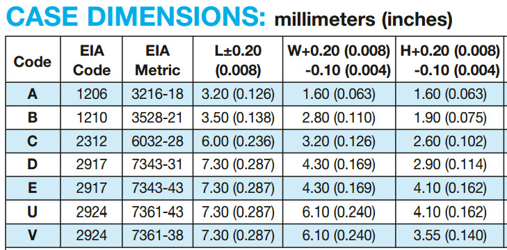
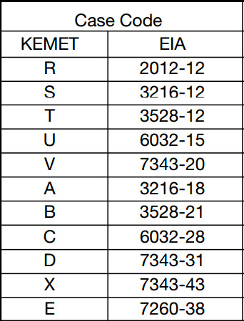
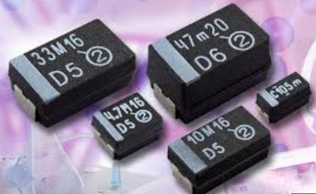
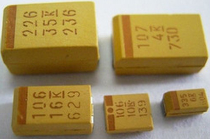
http://www.digikey.com/Web%20Export/Supplier%20Content/Kemet_399/PDF/Kemet_TantalumSMCap.pdf
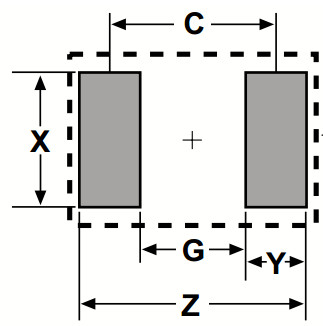
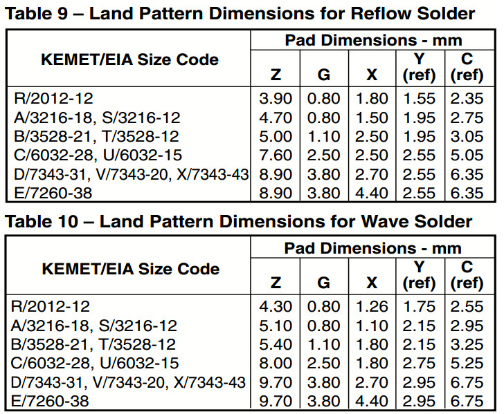
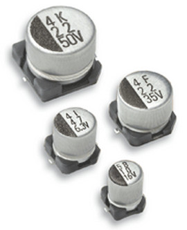
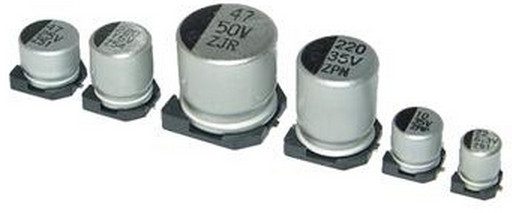
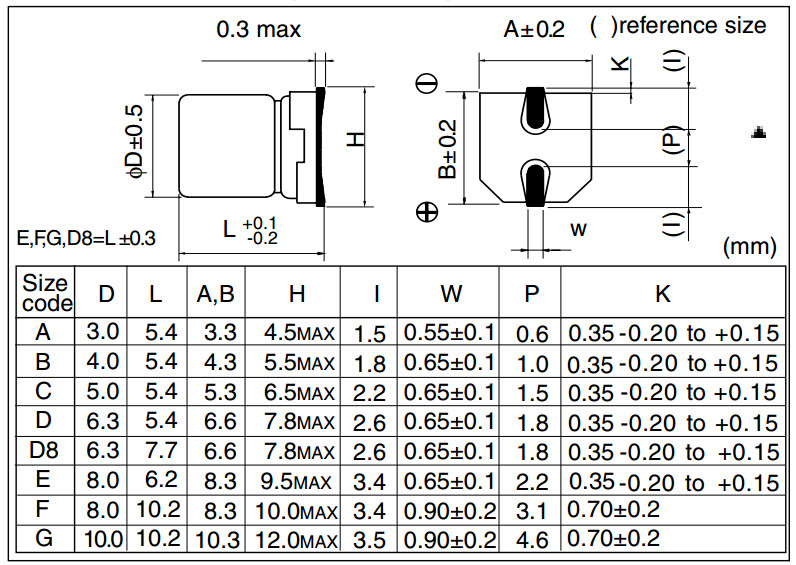
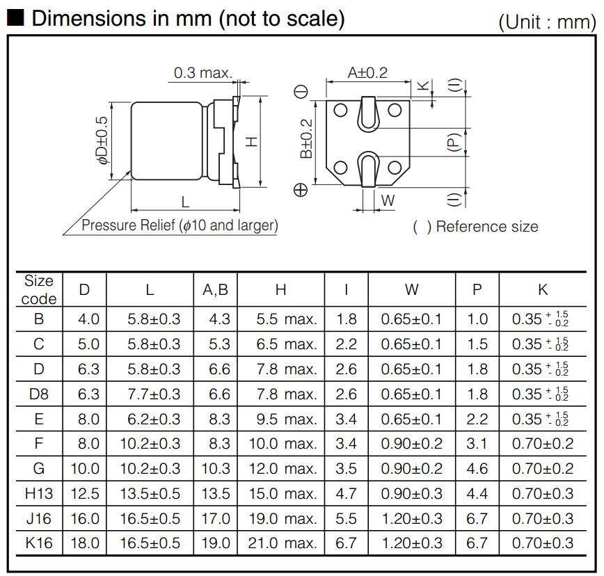
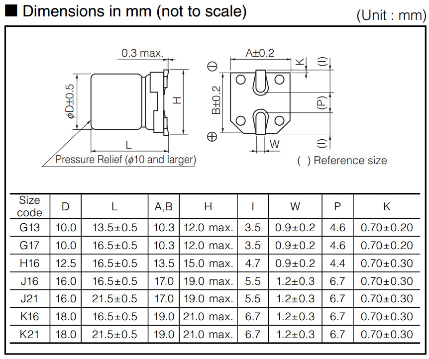
- Aluminium capacitors:[15][16][17]
- (Panasonic A, Chemi-Con B): 3.3 mm × 3.3 mm
- (Panasonic B, Chemi-Con D): 4.3 mm × 4.3 mm
- (Panasonic C, Chemi-Con E): 5.3 mm × 5.3 mm
- (Panasonic D, Chemi-Con F): 6.6 mm × 6.6 mm
- (Panasonic E/F, Chemi-Con H): 8.3 mm × 8.3 mm
- (Panasonic G, Chemi-Con J): 10.3 mm × 10.3 mm
- (Chemi-Con K): 13.0 mm × 13.0 mm
- (Panasonic H): 13.5 mm × 13.5 mm
- (Panasonic J, Chemi-Con L): 17.0 mm × 17.0 mm
- (Panasonic K, Chemi-Con M): 19.0 mm × 19.0 mm
- Power Inductor
- (Panasonic A, Chemi-Con B): 3.3 mm × 3.3 mm
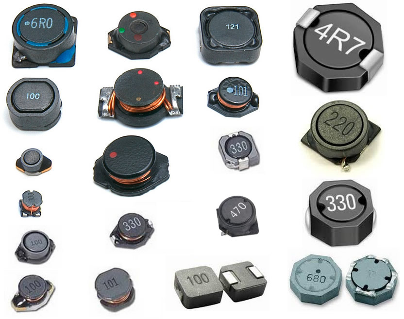
LBS Series SMD Power Inductors
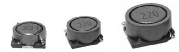
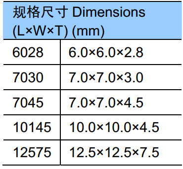
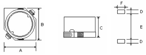
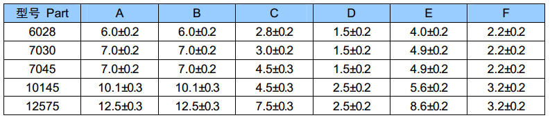
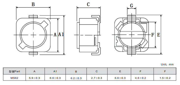
MS Series SMD Power Inductors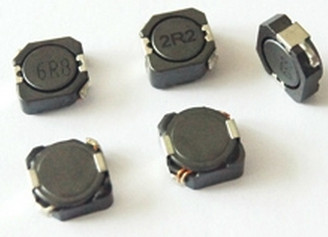
MS103R/104R/105R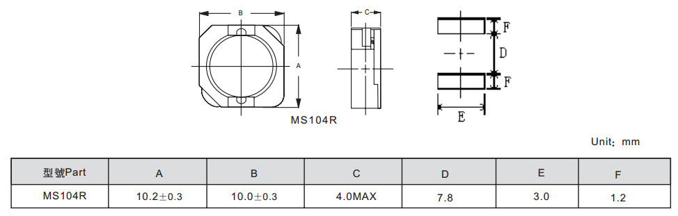
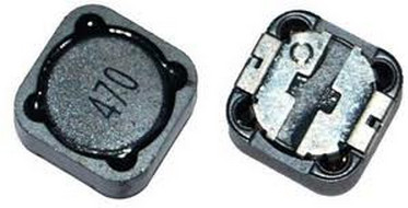
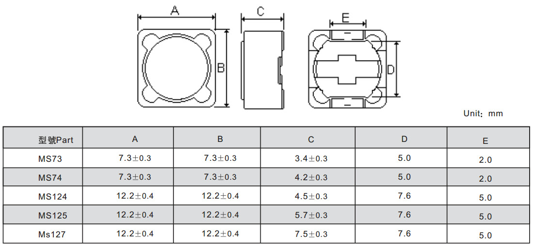
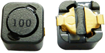
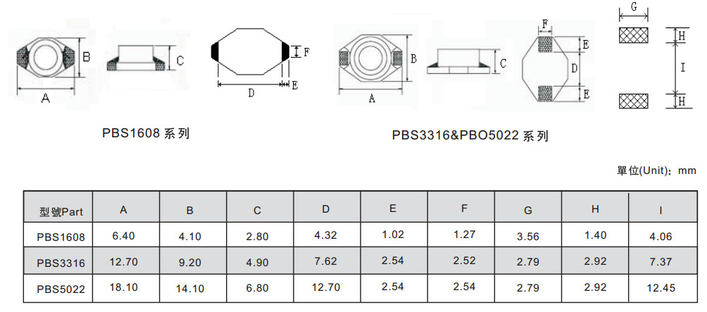
PBS Series SMD Power Inductors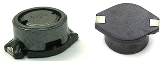
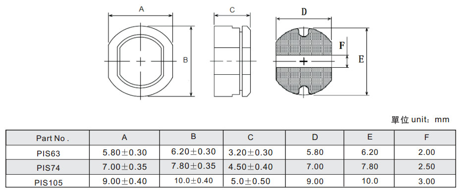
PIS Series SMD Power Inductors
PS-D Series SMD Power Inductors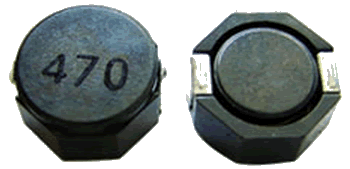
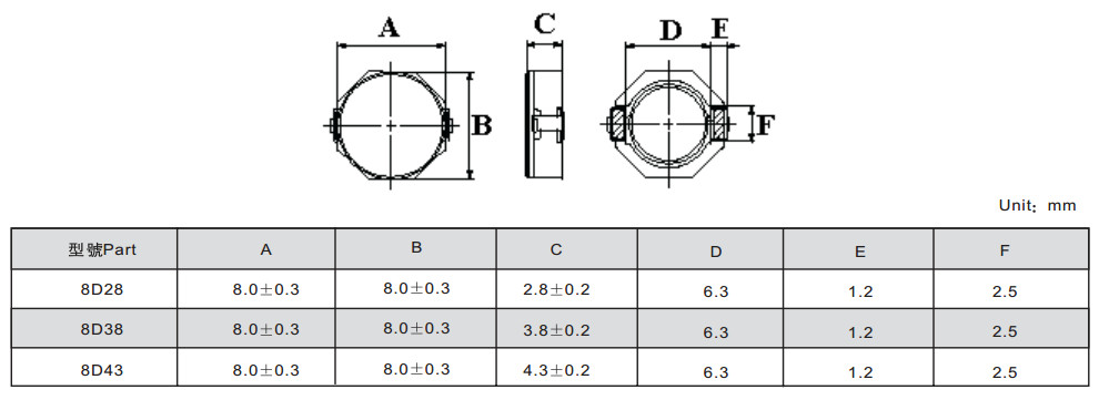
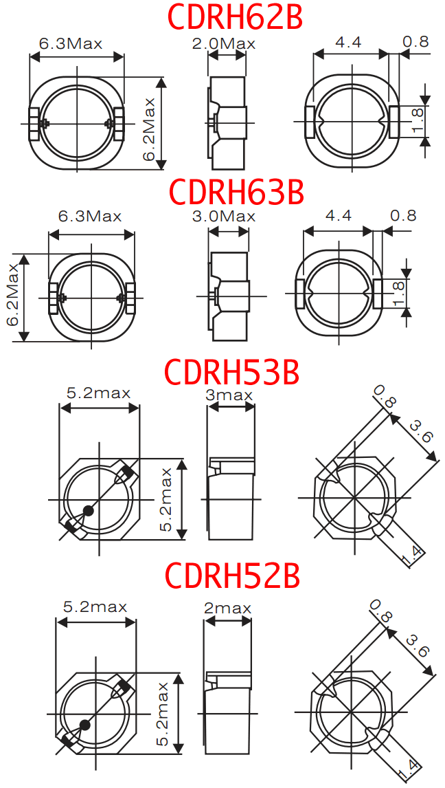

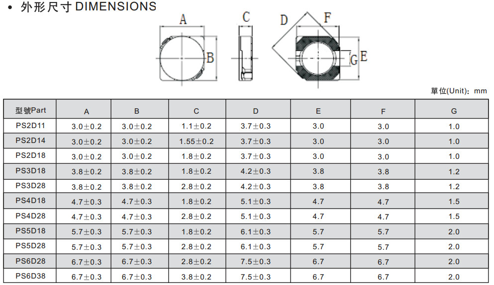
PIO SERIES SMD POWER INDUCTORS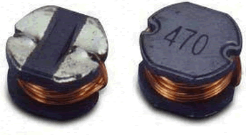
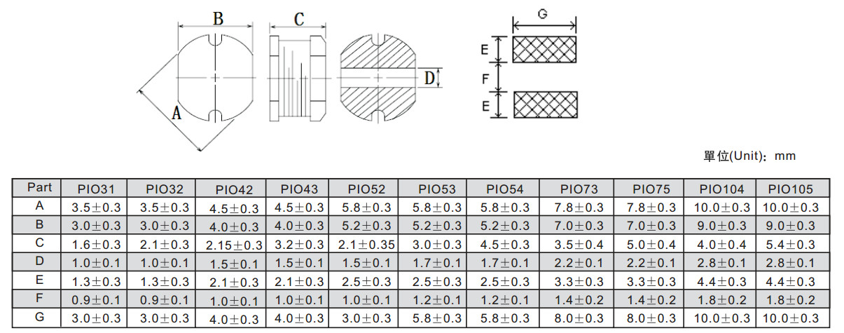
PBO SERIES SMD POWER INDUCTORS
PBO-M SERIES SMD POWER INDUCTORS
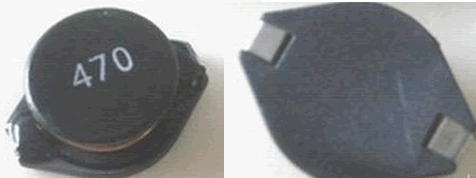
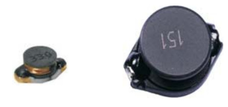
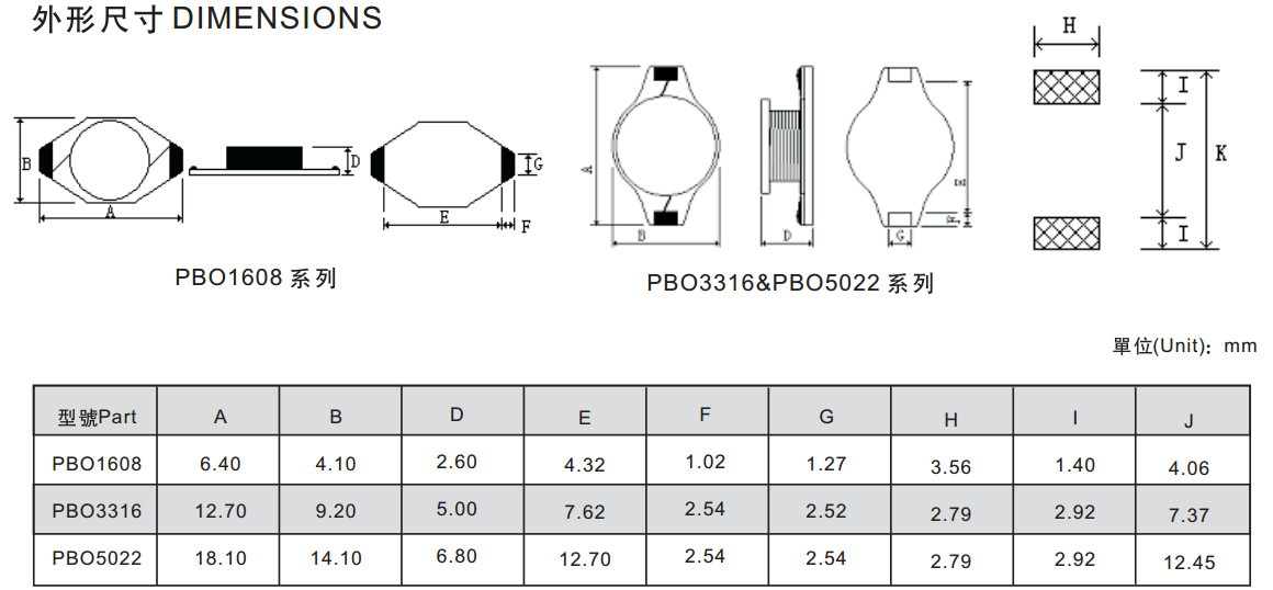
PBO-M SERIES SMD POWER INDUCTORS
- (Panasonic A, Chemi-Con B): 3.3 mm × 3.3 mm
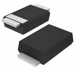
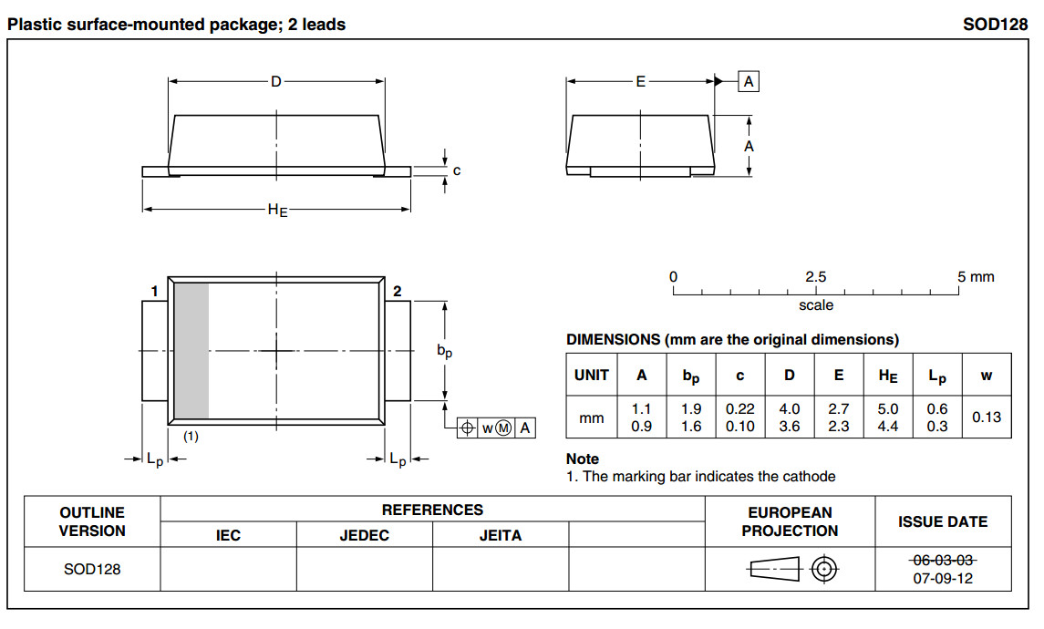
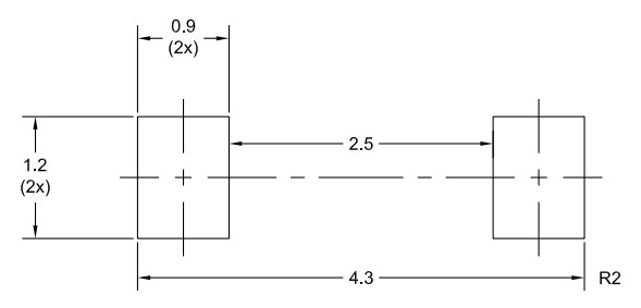
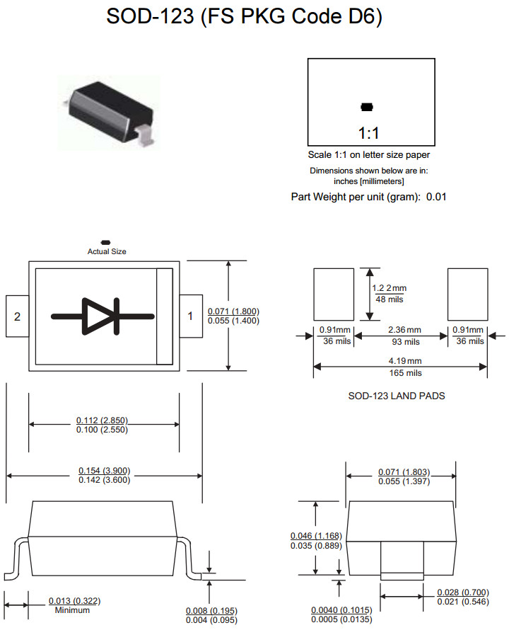
- SOD: Small Outline Diode
http://www.soselectronic.cz/a_info/resource/b/diotec/smd-discretes.pdf
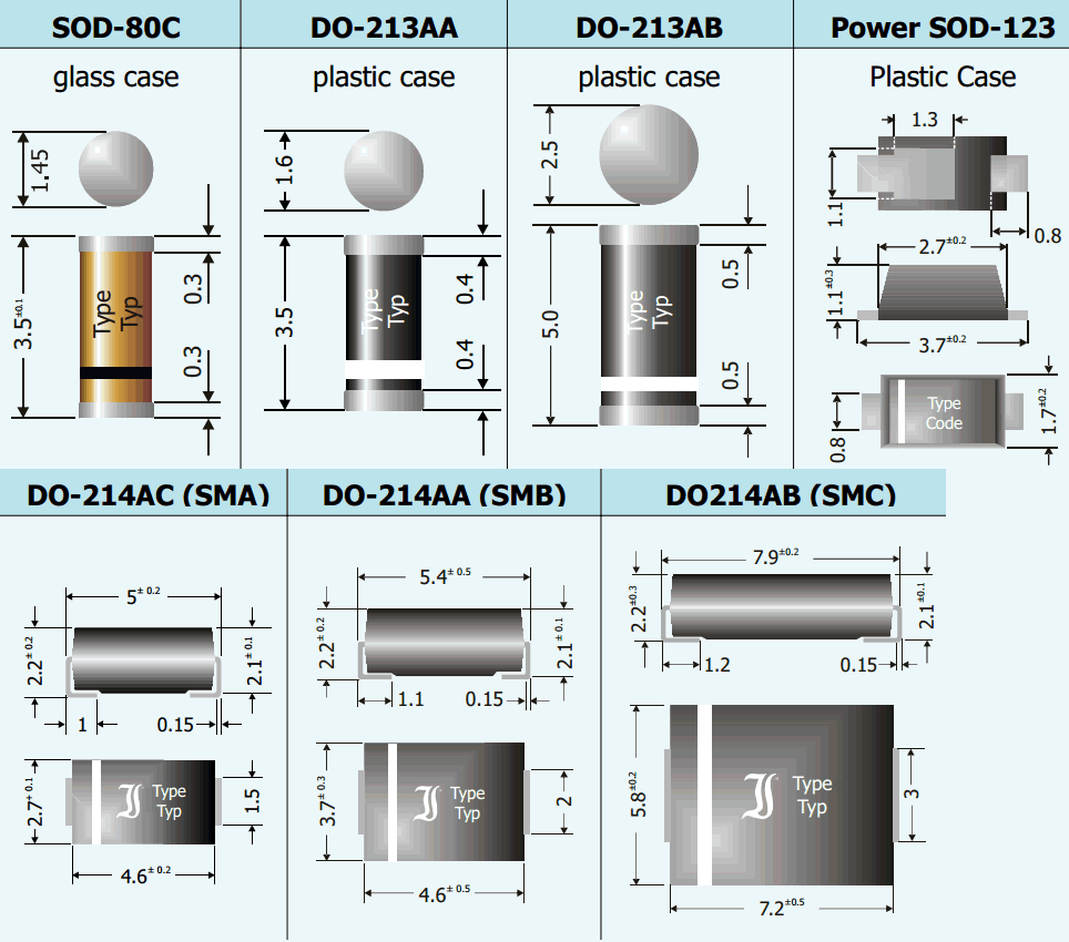
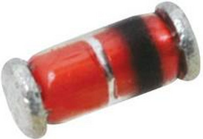
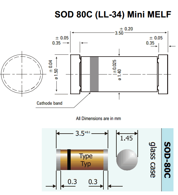
- MELF (Metal Electrode Leadless Face): mostly resistors and diodes; barrel shaped components,
dimensions do not match those of rectangular references for identical codes.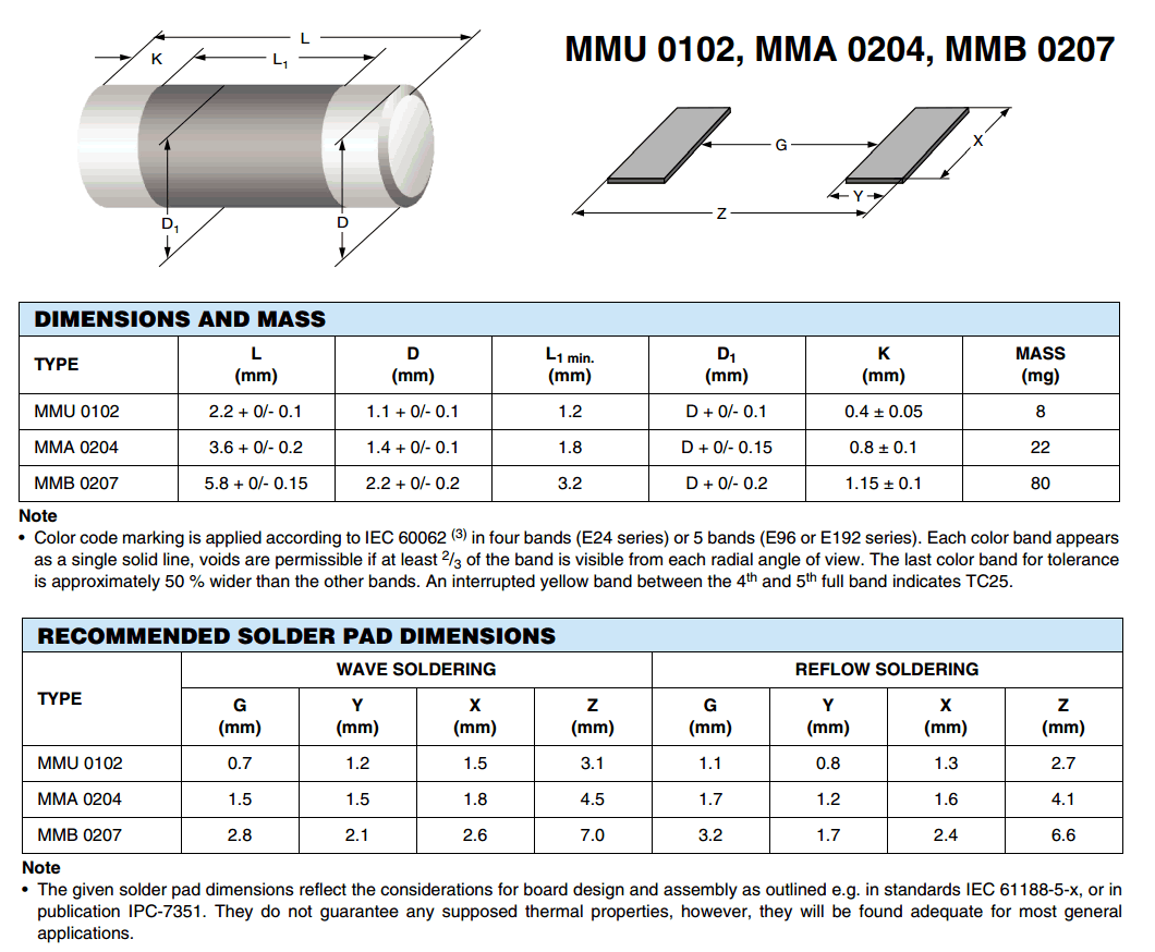
- MicroMelf (MMU) Size 0102: length: 2.2 mm, diam.: 1.1 mm. Typical rating for resistors = 0.2 to 0.3 watt / 150 V[24]
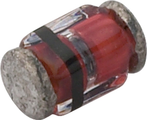
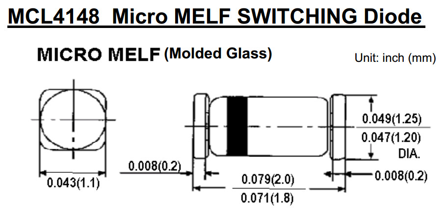
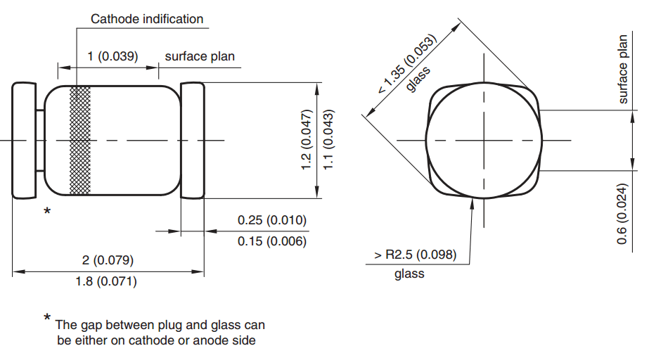
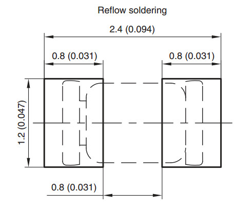
- MiniMelf (MMA) Size 0204: length: 3.6 mm, diam.: :1.4 mm. Typical rating for resistors = 0.25 to 0.4 watt / 200 V[24]
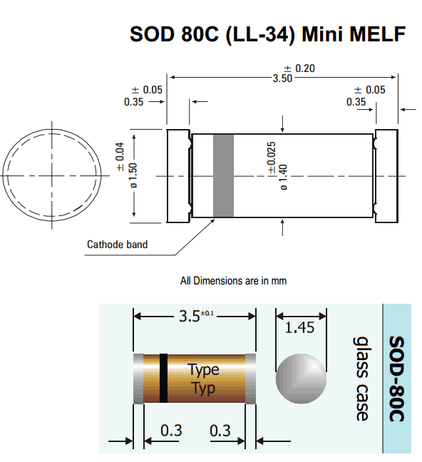
- Melf (MMB) Size 0207: length: 5.8 mm, diam.: 2.2 mm. Typical rating for resistors = 0.4 to 1 watt / 300 V[24]
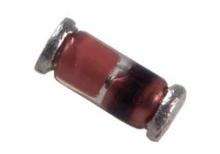
- MicroMelf (MMU) Size 0102: length: 2.2 mm, diam.: 1.1 mm. Typical rating for resistors = 0.2 to 0.3 watt / 150 V[24]
- Rectangular passive components (mostly resistors and capacitors):
- Three-terminal packages
- SOT: Small Outline Transistor, three terminals
- SOT-223 (SC-73): 6.7 mm × 3.7 mm × 1.8 mm body: four terminals, one of which is a large heat-transfer pad [25]
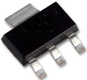
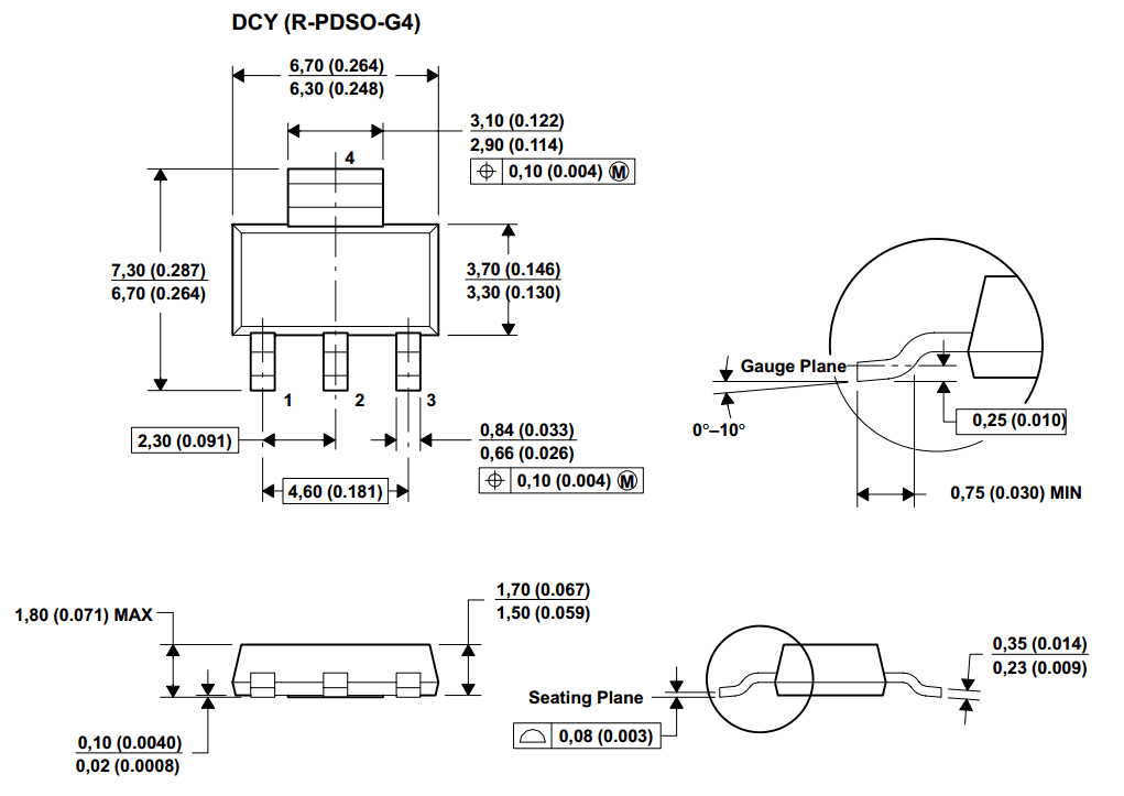
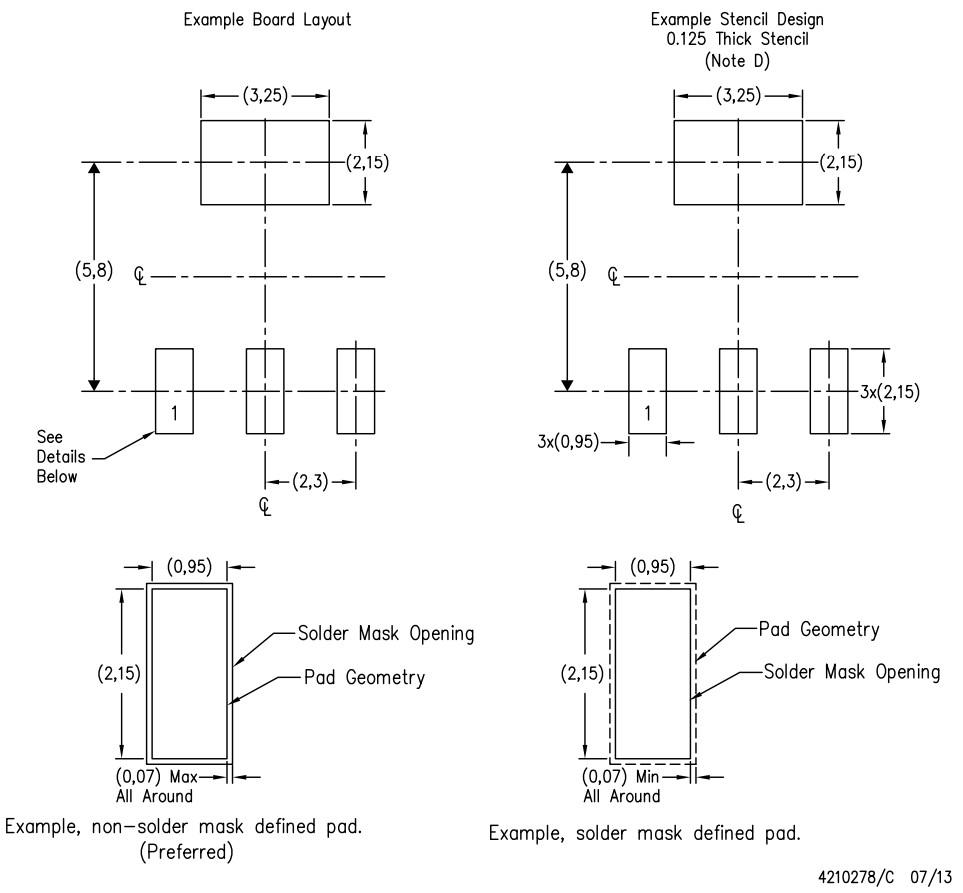
- SOT-223-6
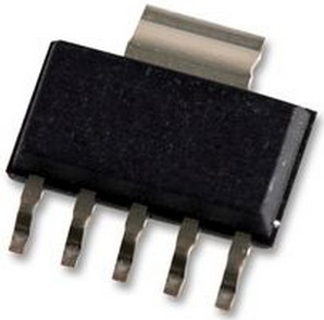
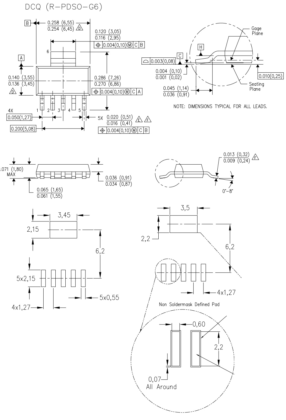
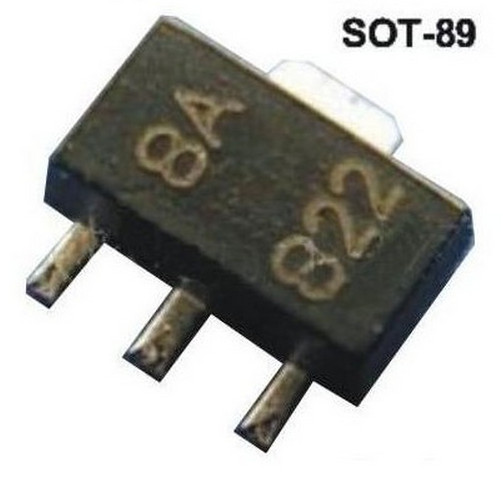
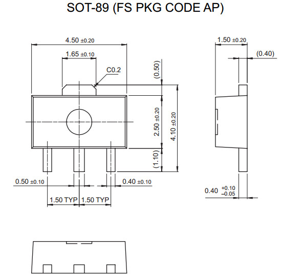
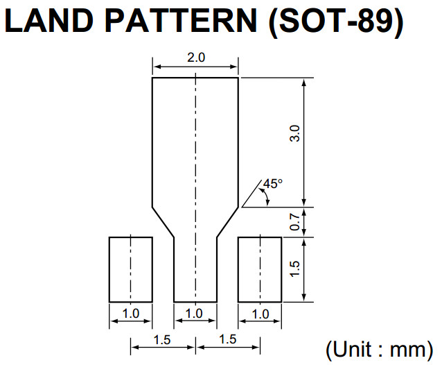
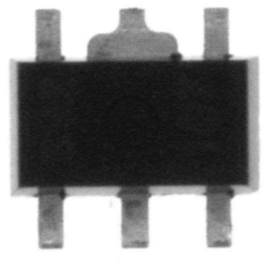
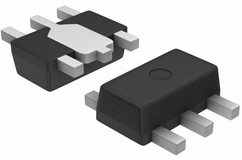
- SOT-89: 4.5 mm × 2.5 mm × 1.5 mm body: four terminals, center pin is connected to a large heat-transfer pad [26]
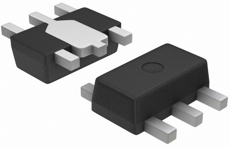
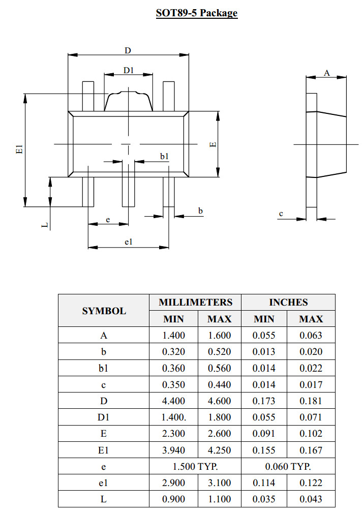
- SOT89-5
- SOT-23 (SC-59, TO-236-3): 2.9 mm × 1.3/1.75 mm × 1.3 mm body: three terminals for a transistor [27]
- SOT-323 (SC-70): 2 mm × 1.25 mm × 0.95 mm body: three terminals [28]
- SOT-416 (SC-75): 1.6 mm × 0.8 mm × 0.8 mm body: three terminals [29]
- SOT-663: 1.6 mm × 1.6 mm × 0.55 mm body: three terminals [30]
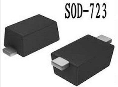
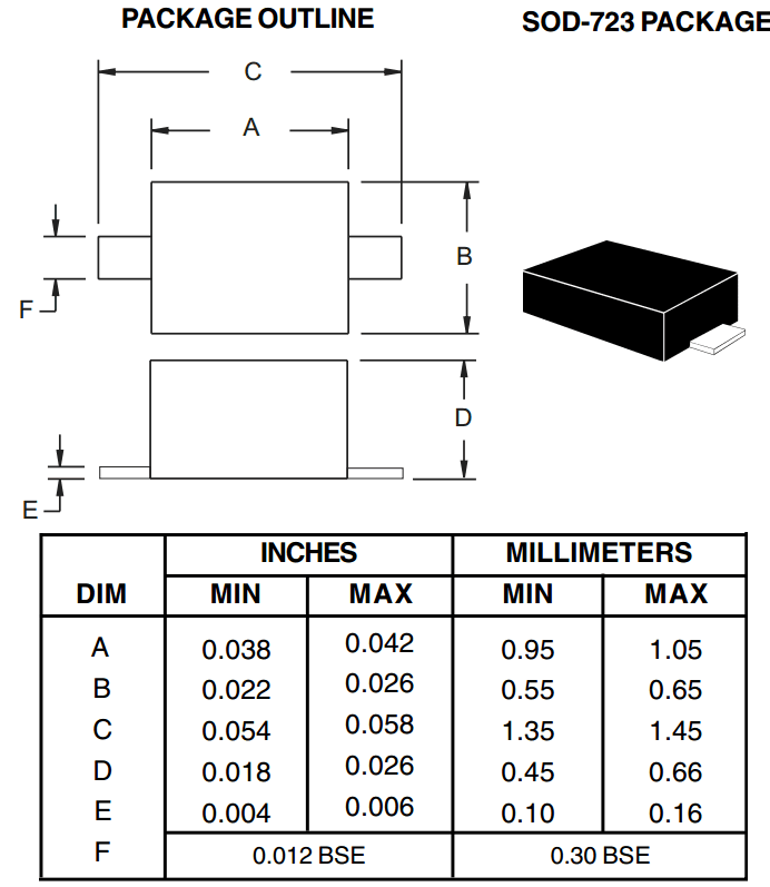
- SOT-723: 1.2 mm × 0.8 mm × 0.5 mm body: three terminals: flat lead[31]
- SOT-883 (SC-101): 1 mm × 0.6 mm × 0.5 mm body: three terminals: leadless [32]
- SOT-223 (SC-73): 6.7 mm × 3.7 mm × 1.8 mm body: four terminals, one of which is a large heat-transfer pad [25]
- DPAK (TO-252, SOT-428): Discrete Packaging.
Developed by Motorola to house higher powered devices. Comes in three- or five-terminal versions [33] - D2PAK (TO-263, SOT-404): bigger than the DPAK;
basically a surface mount equivalent of the TO220 through-hole package.
Comes in 3, 5, 6, 7, 8 or 9-terminal versions [34] - D3PAK (TO-268): even larger than D2PAK [35]
- SOT: Small Outline Transistor, three terminals
- Five- and six-terminal packages
- SOT: small-outline transistor, with more than three terminals
- SOT-23-5 (SOT-25): 2.9 mm × 1.3/1.75 mm × 1.3 mm body: five terminals [36]
- SOT-23-6 (SOT-26): 2.9 mm × 1.3/1.75 mm × 1.3 mm body: six terminals [37]
- SOT-23-8 (SOT-28): 2.9 mm × 1.3/1.75 mm × 1.3 mm body: eight terminals [38]
- SOT-353 (SC-88A): 2 mm × 1.25 mm × 0.95 mm body: five terminals [39]
- SOT-363 (SC-88, SC-70-6): 2 mm × 1.25 mm × 0.95 mm body: six terminals [40]
- SOT-563: 1.6 mm × 1.2 mm × 0.6 mm body: six terminals [41]
- SOT-665: 1.6 mm × 1.6 mm × 0.55 mm body: six terminals [42]
- SOT-666: 1.6 mm × 1.6 mm × 0.55 mm body: six terminals [43]
- SOT-886: 1.5 mm × 1.05 mm × 0.5 mm body: six terminals: leadless
- SOT-886: 1 mm × 1.45 mm × 0.5 mm body: six terminals: leadless [44]
- SOT-891: 1.05 mm × 1.05 mm × 0.5 mm body: five terminals: leadless
- SOT-953: 1 mm × 1 mm × 0.5 mm body: five terminals
- SOT-963: 1 mm × 1 mm × 0.5 mm body: six terminals
- SOT-1115: 0.9 mm × 1 mm × 0.35 mm body: six terminals: leadless [45]
- SOT-1202: 1 mm × 1 mm × 0.35 mm body: six terminals: leadless [46]
- SOT: small-outline transistor, with more than three terminals

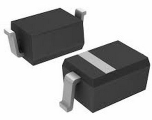
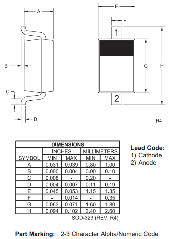
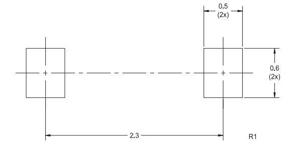
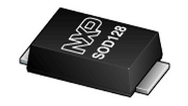


- Packages with more than six terminals[47]
- Dual-in-line
- flatpack was one of the earliest surface-mounted packages.
- SOIC: (Small-Outline Integrated Circuit), dual-in-line, 8 or more pins, gull-wing lead form, pin spacing 1.27 mm
- SOJ: Small-Outline Package, J-Leaded, the same as SOIC except J-leaded [48]
- TSOP: Thin Small-Outline Package, thinner than SOIC with smaller pin spacing of 0.5 mm
- SSOP: Shrink Small-Outline Package, pin spacing of 0.65 mm, sometimes 0.635 mm or in some cases 0.8 mm
- TSSOP: Thin Shrink Small-Outline package.
- QSOP: Quarter-Size Small-Outline package, with pin spacing of 0.635 mm
- VSOP: Very Small Outline Package, even smaller than QSOP; 0.4, 0.5 mm or 0.65 mm pin spacing
- DFN: Dual Flat No-lead, smaller footprint than leaded equivalent
- Quad-in-line
- PLCC: Plastic Leaded Chip Carrier, square, J-lead, pin spacing 1.27 mm
- QFP: Quad Flat Package, various sizes, with pins on all four sides
- LQFP: Low-profile Quad Flat Package, 1.4 mm high, varying sized and pins on all four sides
- PQFP: Plastic Quad Flat-Pack, a square with pins on all four sides, 44 or more pins
- CQFP: Ceramic Quad Flat-Pack, similar to PQFP
- MQFP: Metric Quad Flat Pack, a QFP package with metric pin distribution
- TQFP: Thin Quad Flat Pack, a thinner version of PQFP
- QFN: Quad Flat No-lead, smaller footprint than leaded equivalent
- LCC: Leadless Chip Carrier, contacts are recessed vertically to "wick-in" solder. Common in aviation electronics because of robustness to mechanical vibration.
- MLP (MLF): Micro Leadframe Package (Micro Lead-Frame package) with a 0.5 mm contact pitch, no leads (same as QFN) [49]
- PQFN: Power Quad Flat No-lead, with exposed die-pad[s] for heatsinking
- Grid arrays
- PGA: Pin grid array.
- BGA: Ball Grid Array, with a square or rectangular array of solder balls on one surface, ball spacing typically 1.27 mm
- LGA: An array of bare lands only. Similar to in appearance to QFN, but mating is by spring pins within a socket rather than solder.
- FBGA: Fine pitch Ball Grid Array, with a square or rectangular array of solder balls on one surface
- LFBGA: Low profile Fine pitch Ball Grid Array, with a square or rectangular array of solder balls on one surface, ball spacing typically 0.8 mm
- TFBGA: Thin Fine pitch Ball Grid Array, with a square or rectangular array of solder balls on one surface, ball spacing typically 0.5 mm
- CGA: Column Grid Array, circuit package in which the input and output points are high temperature solder cylinders or columns arranged in a grid pattern.
- CCGA: Ceramic Column Grid Array, circuit package in which the input and output points are high temperature solder cylinders or columns arranged in a grid pattern. The body of the component is ceramic.
- μBGA: micro-BGA, with ball spacing less than 1 mm
- LLP: Lead Less Package, a package with metric pin distribution (0.5 mm pitch).
- Non-packaged devices (although surface-mount, these devices require specific process for assembly):
- COB: Chip-On-Board; a bare silicon chip, that is usually an integrated circuit,
is supplied without a package (usually a lead frame overmolded with epoxy)
and is attached, often with epoxy, directly to a circuit board.
The chip is then wire bonded and protected from mechanical
damage and contamination by an epoxy "glob-top". - COF: Chip-On-Flex; a variation of COB, where a chip is mounted directly to a flex circuit.
- COG: Chip-On-Glass; a variation of COB, where a chip,
typically a Liquid crystal display (LCD) controller, is mounted directly on glass.
- COB: Chip-On-Board; a bare silicon chip, that is usually an integrated circuit,
- Dual-in-line
SMT Surface Mount Technology footprint references的更多相关文章
- Surface Mount Package Details
http://www.centralsemi.com/product/packages/index2.php http://www.infineon.com/cms/cn/product/packag ...
- [转载]Altium规则详解及设置
在Altium中进行PCB的设计时,经常会使用规则(Rule)来进行限定以确定线宽孔径等参数,此文将简要的介绍规则中的一些标量代表了什么. Electrical——电气规则.安全间距,线网连接等 Ro ...
- PCB优化设计(转载)
PCB优化设计(一) 2011-04-25 11:55:36| 分类: PCB设计 目 前SMT技术已经非常成熟,并在电子产品上广泛应用,因此,电子产品设计师有必要了解SMT技术的常识和可制造性 ...
- Altium Designer 规则设置
设计规则设置 Designer Rules Check(DRC) Electrical 电气规则.安全间距,线网连接等 Routing 布线,线宽.过孔形状尺寸.布线拓扑.布线层.封装出线等 SMT ...
- AD16
第三集 制作光敏小夜灯的原理图 1.点击G切换栅格的精度 2.元器件放置好之后要先布局在布线 3.布线完成后要检查电路的合理性.对应查一下电阻的个数,位置是不是符合.在原理上大概的估计是否可以. ...
- The Enginer sample Test for GD temperature control (FCT, ATE, NPI,SMT, )
For me it is a day of grief.................... 1 Communication with customer test methods. notes: T ...
- RFID 仿真/模拟/监控/拦截/检测/嗅探器
Sound card based RFID sniffer/emulator (Too tired after recon.cx to do draw the schematics better th ...
- RFID Reader 线路图收集
This 125 kHz RFID reader http://www.serasidis.gr/circuits/RFID_reader/125kHz_RFID_reader.htm http:// ...
- USBDM RS08/HCS08/HCS12/Coldfire V1,2,3,4/DSC/Kinetis Debugger and Programmer -- MC9S08JS16
Introduction The attached files provide a port of a combined TBDML/OSBDM code to a MC9S08JS16 proces ...
随机推荐
- xshell连接Ubuntu虚拟机
Ubuntu系统 1,安装ssh sudo apt-get install openssh-server 2,启动ssh进程 /etc/init.d/ssh start 3,查看进程信息 ps -e ...
- [转载]FFmpeg完美入门[3] - FFmpeg功能及使用说明
1 ffplay对多媒体的支持能力验证 一.视频3gp 177X144 支持播放,在windows下播放正常,但是在linux下面偶有BUG 如果发现画面无法显示而声音可以播放的情况下可以试着切换全屏 ...
- python使用virtualenv
virtualenv是python的虚拟环境,可以同时存在多个不同的虚拟环境. #1.安装virtualenv pip install virtualenv #2.创建目录 mkdir myproje ...
- vue数据传递--我有特殊的实现技巧
最近碰到了比较多的关于vue的eventBus的问题,之前定技术选型的时候也被问到了,vuex和eventBus的使用范围.所以简单的写一下.同时有一种特殊的实现方案. 有这么几种数据传递方式,vue ...
- 手游研发CJ抱大腿指南
文摘要:CJ来了,又是一年一度的游戏圈盛事,随着手游行业的迅速崛起,今年CJ上,手游研发商以及发行商必定成为焦点.由于门槛低.市场热.前景好等因素的影响,国内一下子蹦出一大堆手游研发团队.很幸运(或者 ...
- POJ 1661 Help Jimmy(二维DP)
题目链接:http://poj.org/problem?id=1661 题目大意: 如图包括多个长度和高度各不相同的平台.地面是最低的平台,高度为零,长度无限. Jimmy老鼠在时刻0从高于所有平台的 ...
- 【转载】python import和from import
import和from import都是将其他模块导入当前模块中. 刚开始一直以为import和from import唯一的区别,就是from import可以少写一些模块名.虽然from XX im ...
- HTML 禁止显示input默认提示信息
看问题 html代码 <!DOCTYPE html> <html lang="en"> <head> <meta charset=&quo ...
- 【转+整理+答案】python315+道面试题
提示 自己整理的答案,很局限,如有需要改进的地方,或者有更好的答案,欢迎提出! [合理利用 Ctrl+F 提高查找效率] 第一部分 Python基础篇(80题) 1.为什么学习Python? # 因为 ...
- Android学习笔记(四) 定时器Timer
Android考虑到线程安全问题,不允许在线程中执行UI线程. 所以在线程中不允许有UI操作 可以利用Handler机制来接收Timer每隔一秒发出的信息,也可以直接利用handler机制的 1.方法 ...