
XuLA/XuLA2
http://www.xess.com/prods/prod048.php XuLA
http://www.xess.com/prods/prod055.php XuLA2

http://www.xess.com/manuals/XuLA-manual.pdf
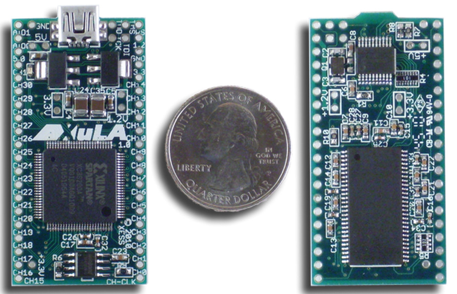

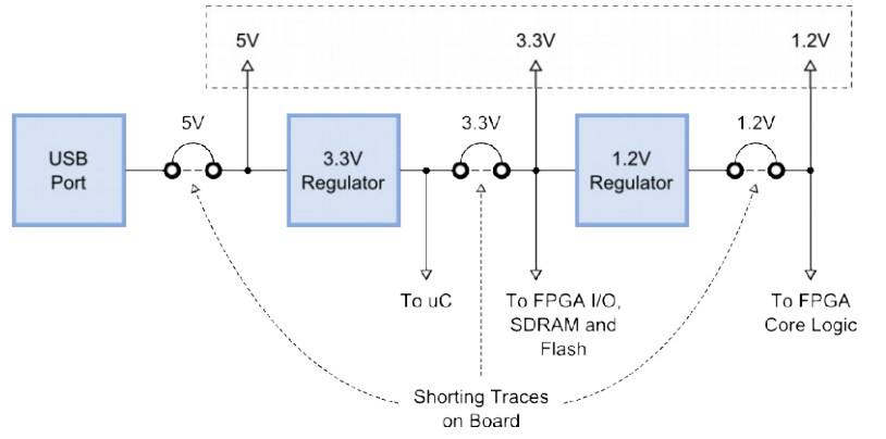
FPGA
The programmable logic device on the XuLA Board is either a XILINX 200,000-gate
XC3S200A Spartan 3A FPGA in a 100-pin VQFP, or a 50,000-gate XC3S50A.
Microcontroller
The XuLA Board uses a Microchip 18F14K50 PIC to perform the following functions:
Reset & initialization: Upon power-up or assertion of the reset, the microcontroller
initiates the configuration of the FPGA from the Flash and holds the FPGA in its
cleared state if the configuration fails. It instantiates its USB endpoints and
participates in the USB enumeration process.
Clock generation: The microcontroller uses its pulse-width modulation (PWM) circuitry
to generate a 12 MHz square-wave that enters one of the FPGA's global clock
inputs.
USB-to-JTAG communication: The microcontroller accepts configuration bitstreams and
data as packets over the USB link and transforms these into a sequence of
transitions upon the FPGA's JTAG pins. It also receives data from the FPGA
through the JTAG port which it bundles into packets for return through the USB
link.
SDRAM
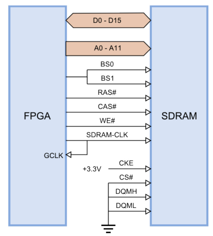
The XuLA Board incorporates an 8M x 16 SDRAM (Winbond W9812G6JH) that connects to
the FPGA as shown below. To compensate for circuit delays, the clock signal to the
SDRAM is re-routed back to a global clock input so the FPGA can synchronize itself with
the SDRAM.
Because of the limited number of pins provided by the FPGA's package, the following
modifications were made to the SDRAM interface:
The chip-select (CS#) is tied low so the SDRAM is always enabled.
The clock-enable (CKE) is tied high so the SDRAM always requires a clock signal in
order to keep its data refreshed.
Both data qualifier mask enables (DQMH and DQML) are tied low to disable byte-wide
access to the SDRAM, so all operations involve the entire sixteen-bit data width.
A single FPGA pin drives both bank-select inputs (BS0 and BS1). This reduces the
accessible region of the SDRAM by half to 4M x 16.
Flash
The XuLA Board has a 2-Mbit SPI Flash (Winbond W25X20BV) that connects to the FPGA
as shown below.
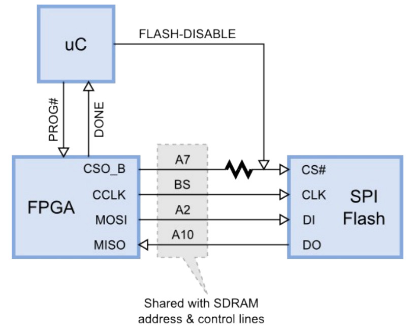
Due to the limited I/O of the FPGA package, the Flash and SDRAM chips share some of
the FPGA pins. In combination with the SDRAM being permanently enabled (its chip-select
is always asserted), this means that the Flash and SDRAM cannot be used simultaneously.
Therefore, the following events occur when the XuLA Board comes on:
1. The microcontroller puts its FLASH-DISABLE output into a high impedance state and
pulses the FPGA's PROG# pin to initiate the configuration from the Flash.
2. The FPGA lowers its CSO_B pin to enable the Flash, and then uses its CCLK, MOSI and
MISO pins to read the stored bitstream. Because the SDRAM is not active during the
FPGA's configuration (SDRAM-CLK is inactive since the FPGA is not configured), it
doesn't matter if the SDRAM address and control pins are toggling.
3. Once the Flash delivers its bitstream, the FPGA's DONE pin is asserted. The
microcontroller senses this and drives its output pin high to de-assert the FLASHDISABLE signal,
thus turning the Flash off. The FPGA can't access the Flash any more,
but it can access the SDRAM without affecting the Flash.
It is possible to set a flag that prevents the microcontroller from disabling the Flash after
the FPGA is configured (as described here). Then the logic design loaded into the FPGA
can access the Flash, but it can no longer use the SDRAM (the toggling of the SDRAM
address and control pins might inadvertently corrupt the Flash contents).
5V Tolerance Issues
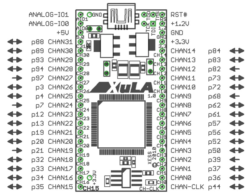
The CHAN* and CHAN-CLK pins connect directly to the pins of the FPGA which typically
use an I/O voltage of 3.3V. When driving the inputs of external 5V logic, you should check
that their VIH threshold is less than the VOH of the XuLA outputs. (This is true for most 5V
logic families.)
You must also take care not to exceed the input voltage rating of the FPGA pins when
they are driven by external 5V logic outputs. A common technique for protecting the
Xilinx FPGA pins is shown below. When presented with a voltage greater than 3.3V + 0.7V
= 4.0V, the protection diode built into the FPGA pin's circuitry conducts current and the
excess voltage is dropped across the 100Ω resistor. This keeps the voltage directly on the
FPGA pin from ever exceeding 4V, which is within tolerated limits. The resistor value
should be set so the current through the protection diode does not exceed 10 mA.
However, by default, the Xilinx Spartan-3A FPGA disables the protection diodes.
In order to enable these diodes, you can place the following text into your Xilinx ISE
project constraint file for every I/O pin that will be connected to 5V logic:
NET "input_name" IOSTANDARD = PCI66_3;

http://www.xess.com/manuals/XuLA2-manual.pdf
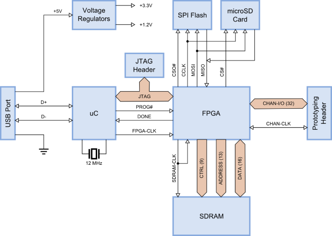
XuLA2 is an open-source FPGA development board, based on Xilinx Spartan-6 LX25 low cost FPGA.
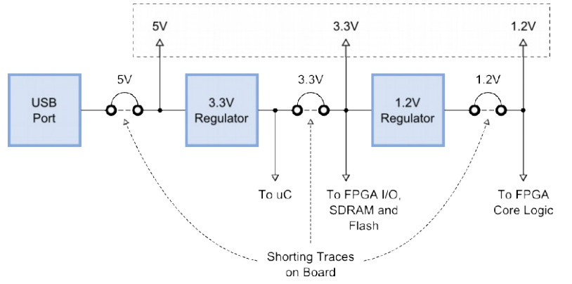
The design provides 32MB SDRAM, micro-SD card slot, two voltage regulators, supervisory circuitry
based on PIC 18F14K50 microcontroller and USB port for programming the FPGA.


FPGA
The programmable logic device on the XuLA2 is a XILINX XC6SLX25 Spartan 6 FPGA in a
256-ball BGA package (FT256).
Microcontroller
The XuLA2 uses a Microchip 18F14K50 PIC to perform the following functions:
Reset & initialization: Upon power-up or assertion of the reset, the microcontroller
initiates the configuration of the FPGA from the SPI Flash and holds the FPGA in
its cleared state if the configuration fails. It instantiates its USB endpoints and
participates in the USB enumeration process.
Clock generation: The microcontroller uses its pulse-width modulation (PWM) circuitry
to generate a 12 MHz square-wave that enters one of the FPGA's global clock
inputs.
USB-to-JTAG communication: The microcontroller accepts configuration bitstreams and
data as packets over the USB link and transforms these into a sequence of
transitions upon the FPGA's JTAG pins. It also receives data from the FPGA
through the JTAG port which it bundles into packets for return through the USB
link.
SDRAM
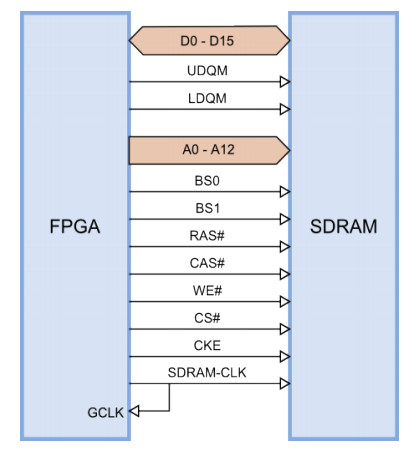
The XuLA2 incorporates a 16M x 16 SDRAM (Winbond W9825G6JH) that connects to the
FPGA as shown below. To compensate for circuit delays, the clock signal to the SDRAM is
re-routed back to a global clock input so the FPGA can synchronize itself with the SDRAM.
SPI Flash and microSD Card
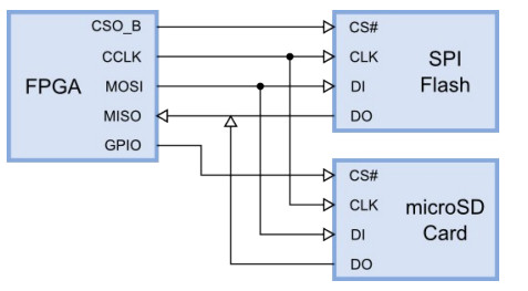
The XuLA2 has an 8-Mbit SPI Flash (Winbond W25Q80BV) and a microSD card socket that
connect to the FPGA as shown below. During FPGA configuration, the bitstream is read
from the SPI flash while the microSD card is disabled. After configuration, either the SPI
Flash or the microSD card can be accessed by lowering their respective chip-selects and
performing SPI read/write operations.
XuLA/XuLA2的更多相关文章
- Unity3D|-XLua热更新用法的大致流程
xlua是由腾讯维护的一个开源项目,我们可以在github上下载这个开源项目并查看一些相关文档 官网:https://github.com/Tencent/xLua 配置文档:https://gith ...
- miniSpartan6, another Spartan 6 Kit
http://thehardwarer.com/2013/05/minispartan-6-another-spartan-6-kit/ miniSpartan6 is an Opens Source ...
随机推荐
- JSOI 2017 退役记
意料之中,真的要退役了. 懒得写游记了. Round 2 的时候状态一直不太清醒,最后混了个rank19,准备AFO吧.
- 关于ORA-04091异常的出现原因,以及解决方案
问题分析 在Oracle中执行DML语句的时候是需要显示进行提交操作的.当我们进行插入的时候,会触发触发器执行对触发器作用表和扩展表的种种操作,但是这个时 候触发器和插入语句是在同一个事务管理中的,因 ...
- HTML文件编码
为了防止中文乱码,一般在网页头文件中加入 <meta http-equiv="Content-Type" content="text/html; charset=u ...
- bzoj 2819(DFS序+树状数组+博弈+lca)
2819: Nim Time Limit: 20 Sec Memory Limit: 128 MBSubmit: 2045 Solved: 795[Submit][Status][Discuss] ...
- python实现IMAP协议下email收取
本文为转载,原文在这里. 所谓无痕取信,目前主要是指从邮箱中把信件收取后,邮箱内状态不发生任何改变.这里的状态主要是指两部分,一部分是邮件状态不变,即已读与未读状态不变,另一部分是指邮箱记录的登陆IP ...
- 关于HTML&CSS的笔记
最近在看Jon Duckett的HTML&CSS一书(http://book.douban.com/subject/6585090/),书的排版和讲解方式很不错,并且有许多其他教学材料遗漏的关 ...
- pymongo的一些操作
参考:http://www.yiibai.com/mongodb/mongodb_drop_collection.html http://www.cnblogs.com/zhouxuchen/p/55 ...
- jquery 上传图片自由截取
为了使用户能自定义个人头像,需要提供一个对上传图片的截图功能,当前很多网站特别是SNS类网站都提供这样的功能,非常实用.本文主要是利用jQuery的imgAreaSelect插件实现. 首先引入三个文 ...
- poj2078 Matrix(DFS)
题目链接 http://poj.org/problem?id=2078 题意 输入一个n×n的矩阵,可以对矩阵的每行进行任意次的循环右移操作,行的每一次右移后,计算矩阵中每一列的和的最大值,输出这些最 ...
- C++的一道变态题
题目大概是这样的:有两个数组a[N],b[N],求构造 b[i]=a[0]*a[1]*a[2]*...a[N-1]/a[i], 要求: .不能使用除法. .空间复杂度O(1),时间复杂度O(n). . ...