LPC1800 and LPC4300 Boot/ISP/CRP
MCU的启动方式有很多种:UART接口,扩展的静态存储单元(NOR Flash),
SPI Flash,quad SPI Flash,高速USB0和USB1.另外可以通过对OTP存储单元的编程。
首先看下内存映射:
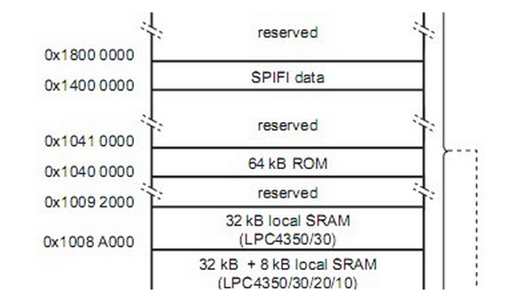
在MCU复位之后,ARM处理器将会从ROM区域执行代码。
LPC43XX包含一个隐藏指针允许内存区域映射到地址0x00000000.
隐藏指针的默认值为0x1040 0000,保证了启动ROM中的代码在复位的时候被执行。
如果启动方式从flash区域开始,那么系统默认会从内部flash启动(引脚p2_7为高)。
如果p2_7引脚在复位的时候取样为低,启动方式将由OTP的 BOOT_SRC位 的设置
或者引脚P2_9,P2_8,P1_2,P1_1的状态而定。
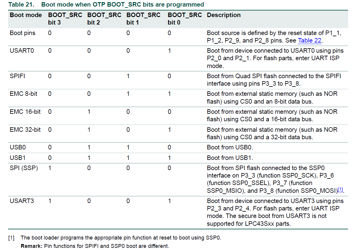
如果BOOT_SRC位被设置,根据值的不同启动的方式不同:
注意:
OTP内存区域属于一次性编程性质,一旦用户在某一程序中设定了其中的值,
那么系统的启动方式就确定了,不能再次进行更改,这个部分一定要注意。
否则,有可能会因为启动方式的定性而导致后续编程的不方便。
如果p2_7引脚在复位的时候取样为低, OTP内存没有经过编程[1111] 或者BOOT_SRC位为 [0000]
启动模式由引脚P2_9,P2_8,P1_2,P1_1的状态决定。
When programming and running code from the external flash, it is particularly important to make sure that
you have the boot pins P2_9, P2_8, P1_2, and P1_1 are correctly connected so that the MCU starts execution from the correct memory address.
For more details, please see the NXP documentation.
If the boot pins are incorrectly set, then this will typically result in the initial default breakpoint set by the debugger on main() not been reached.
You can confirm if this is the case by clicking on suspend icon to pause execution (when you fail to hit the initial breakpoint)
and then looking at the address of the PC.
If you built for SPIFI, then the address of the PC should be 0x14xx xxxx,
whereas if you built for EMC (SST), then the address of the PC should be0x1Cxx xxxx.
BOOT pins example (Hitex LPC1850/4350 board)
For example, for the Hitex LPC1850/4350 board, you need to have the BOOT jumpers configued as follows :
For SPIFI flash
- BOOT1 connected across pins 1 and 2
- BOOT2, BOOT3, BOOT4 connected across pins 2 and 3
For EMC SST flash
- BOOT1, BOOT2 connected across pins 1 and 2
- BOOT3, BOOT4 connected across pins 2 and 3
Note :
A power on reset is definitely required after changing the BOOT pin settings.
The boot ROM memory includes the following features:
• ROM memory size is 64 kB.
• Supports booting from UART interfaces, external static memory such as NOR flash, SPI flash, quad SPI flash, high-speed USB (USB0), and USB1.
• Includes API for OTP programming.
• Includes USB drivers.
• ISP mode for loading data to on-chip SRAM and execute code from this location.
The internal ROM memory is used to store the boot code.
After a reset, the ARM processor will start its code execution from this memory.
The ARM core is configured to start executing code, upon reset, with the program counter being set to the value 0x0000 0000.
The LPC43xx contains a shadow pointer that allows areas of memory to be mapped to address 0x0000 0000.
The default value of the shadow pointer is 0x1040 0000, ensuring that the code contained in the boot ROM is executed at reset.
For flash-based parts, the part boots from internal flash by default (boot pin P2_7 is HIGH).
If the boot pin is sampled LOW on reset, the boot source is determined
by the setting of the OTP or the states of pins P2_9, P2_8, P1_2, and P1_1.
For details of the boot process for flash-based parts, see Figure 13.
For flash-based and flashless parts alike, several external sources are available for booting depending
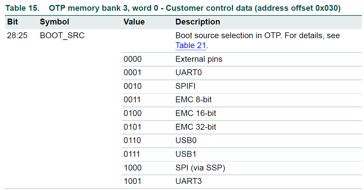
on the values of the OTP bits BOOT_SRC (see Section 4.4).
If the OTP memory is not programmed or the BOOT_SRC bits are all zero,
the boot mode is determined by the states of the boot pins P2_9, P2_8, P1_2, and P1_1.
OTP BOOT_SRC = 0000 : uses External Pins
BOOT_SRC = 0000 : uses External Pins -- Programmed
BOOT_SRC = 1111 : uses External Pins -- Unprogrammed
BOOT_SRC = 0000 : uses External Pins

Set the boot mode jumpers to USB0: BOOT[0:3] = "1010".
P1_1 = BOOT[0], P1_1 = BOOT[1], P2_8 = BOOT[2], P2_9 = BOOT[3]
P2_7 = 0 : ISP < USART0 or USART3 >
Boot process for parts with internal flash
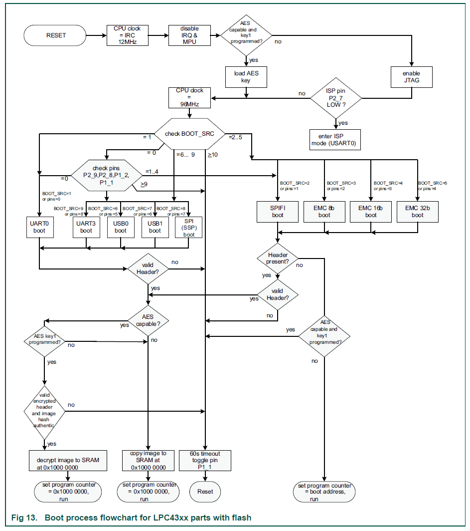
Parts with flash boot from on-chip flash if PIO2_7 is sampled HIGH. See Figure 13.
If pin P2_7 is sampled LOW, the boot loader checks the OTP bits
and/or the external boot pins to determine the communication port.
If the OTP bits and boot pins are set to USART0 or USART3, the part enters UART ISP mode.
A boot image must have a valid signature to be a valid flash image (see Section 6.4.4.1 “Criterion for Valid User Code”),
and on parts with dual flash banks, only one flash bank should contain a valid image.
You can use the ISP/IAP command Set active boot flash bank to configure one flash bank
with the valid image (see Section 6.8.12 and Section 6.7.15).
If both images are valid, the boot loader loads the image located in flash bank A.
Remark:
If the boot loader image is located in flash bank B and data is stored in flash bank A,
then ensure that the data in flash bank A does not appear to be a valid image.
An example of a data set that would be interpreted as a valid image is a set in which the first eight words of flash bank A contain all zeros.
This implies that the data in the first 8 locations of sector 0 in flash bank A cannot be chosen freely.
For example, choose data in location 8 in such a way that a non-valid image is created. See Section 6.4.4.1 “Criterion for Valid User Code”.
Boot process for parts without flash

The top level boot process is illustrated in Figure 14.
The boot starts after Reset is released.
The IRC is selected as CPU clock,the Cortex-M4 starts the boot loader, and JTAG access is enabled.
As shown in Figure 14, the boot ROM determines the boot mode based on the OTP BOOT_SRC value
or reset state of the pins P1_1, P1_2, P2_8, and P2_9.
The boot ROM copies the image to internal SRAM at location 0x1000 0000
and jumps to that location (it sets ARM's to 0x1000 0000) after image verification.
Hence the images for LPC43xx should be compiled with entry point at 0x0000 0000.
On AES capable parts with a programmed AES key, the image and header
are authenticated using the CMAC algorithm prior to copying to the internal SRAM.
If authentication fails the device is reset.
On non-secure parts, the image and header are not authenticated.
If the image is not preceded by a header then the image is not copied to SRAM but assumed to be executable as-is.
In that case the shadow pointer is set to the first address location of the external boot memory.
The header-less images should be compiled with entry point at 0x0000 0000, the same as for an image with header.
Remark:
When the boot process fails, pin P1_1 toggles at a 1 Hz rate for 60 seconds.
After 60 seconds, the device is reset.
Jellybean Notes
A 12 MHz clock signal must be supplied to the LPC4330 at boot time.
"This boot mode requires that a 12 MHz external crystal is connected to the XTAL1/2 pins."
The April 16, 2012 Jellybean design has a voltage divider for VBUS that is fed to the LPC43xx
to detect that a USB host is present.
Measuring the divided voltage, the USB0_VBUS only reaches 0.4V,
which fails to trip the USB bootloader code.
It looks like NXP's intent is to directly connect VBUS to the USB0_VBUS.
Indeed, when I shorted R10 with tweezers, the USB bootloader sprung into action.
I would recommend changing R10 to 0 Ohms and R11 to DNP, or removing R10 and R11 altogether.
DFU/USB boot board configurations
To use DFU/USB boot with the LPC18xx/43xx devices, the chip needs to be configured with the boot jumpers for DFU/USB boot.
LPC18xx/43xx devices can boot via the USB0 or USB1 port.
Hitex 1850 and 4350 board
To setup the Hitex 1850 or 4350 boards for USB DFU boot mode,
configure the BOOT1 - BOOT4 jumpers as follows:
- BOOT1 pins 1-2
- BOOT2 pins 3-4
- BOOT3 pins 1-2
- BOOT4 pins 3-4
Plug the USB cable into the USB0 connector for DFU boot.
Keil MCB1857 and MCB4357 boards
The MCB1857 and MCB4357 boards have devices with internal FLASH and ISP/IAP support.
To setup the board for USB DFU boot mode, reset the board while holding down the ISP button.
Plug the USB cable into the USB0 connector for DFU boot.
NGX Xplorer 1830 and 4330 boards
To setup the NGX Xplorer 1830 and 4330 boards for USB DFU boot mode,
configure the DIP switch block on J4 as follows:
- 1 - Off
- 2 - On
- 3 - Off
- 4 - On
Plug the USB cable into the USB0 connector for DFU boot.
LPC-Link 2 boards : LPC4370 - No Internal Flash
To setup the LPCLink2 boards for USB DFU boot mode, make sure jumper JP1 is open.
LPCXpresso boards with the Link2 DFU boards
To setup the LPCXpresso boards with the integrated Link2 DFU interface for USB DFU boot mode, make sure jumper ;LINK DFU' is closed.
In-System Programming of LPC18xx/43xx flash
This application note provides an overview of In-System programming (ISP) and easy steps
to program the on-chip flash of LPC18xx/43xx flash based Cortex M3/Cortex M4 microcontrollers using Flash Magic software.
Keil’s MCB4300 evaluation board is used for demonstration purposes.
LPC18xx/43xx flash-based chips contain up to 1 MB flash divided into two banks:
• Bank A: 0x1A00 0000 (512 KB max.)
• Bank B: 0x1B00 0000 (512 MB max.)
In an LPC18xx/43xx with on-chip flash, USART0 or USART3 can be used for ISP communication
depending on the OTP bits and/or boot pins.
If all boot pins are held low, USART0 is selected.
In-system programming (ISP) via USART0 is used for this demo with the following pin configuration:
• P2_0 FUNCTION 1, USART0 TXD
• P2_1 FUNCTION 1, USART0 RXD
ISP mode can be entered using pin P2_7 pulled low (GND) before RESET.
LPC43xx USB DFU Notes
The LPC43xx contains USB DFU bootloader support in ROM.
By selecting the appropriate boot mode (USB0), the device will come up on USB at power-up or reset,
and implement the popular and well-documented USB DFU protocol.
Setup
Boot Mode Jumpers
Set the boot mode jumpers to USB0:
BOOT[0:3] = "1010".
Jumper setting takes effect at the next power-on or reset.
(You can rig up a reset button to P2 "LPC_JTAG" or P14 "LPC_ISP".)
USB DFU Utility
You need the latest source from git for some reason.
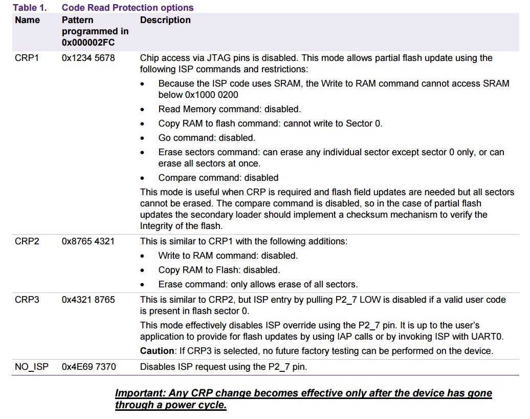
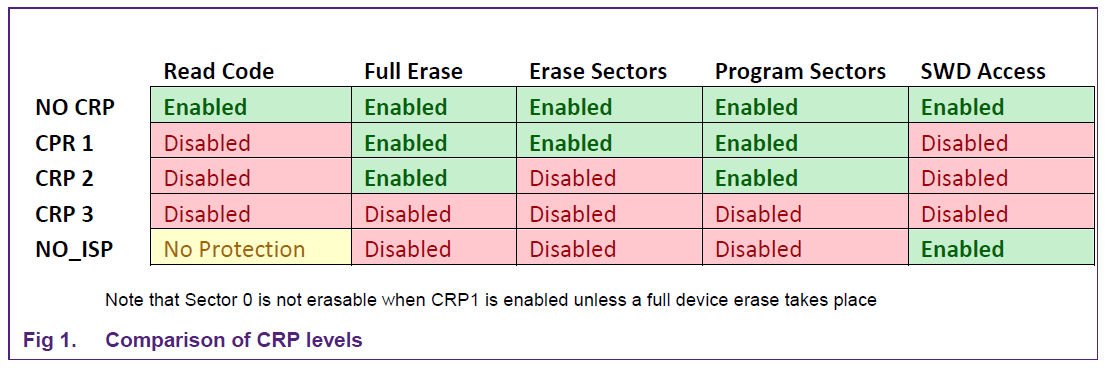
Implications of Code Read Protection (CRP) on flash
Code Read Protection is the mechanism to restrict the access to on-chip flash and ISP.
The demo does not use CRP for simplicity – check ‘Asm’ tab in Target Options.
CRP is invoked by programming a specific pattern in flash at 0x2FC.
There are four different levels of CRP security defined for LPC18xx/43xx which are defined in Table 1:
LPC1800 and LPC4300 Boot/ISP/CRP的更多相关文章
- LPC1800 and LPC4300 MCUs
LPC1800 Series microcontrollers At 180 MHz, LPC1800 Series microcontrollers combine the industry's f ...
- LPCScrypt, DFUSec : USB FLASH download, programming, and security tool, LPC-Link 2 Configuration tool, Firmware Programming
What does this tool do? The LPC18xx/43xx DFUSec utility is a Windows PC tool that provides support f ...
- LPC-LINK 2
LPC-Link 2 is an extensible, stand-alone debug adapter that can be configured to support various dev ...
- NXP LPC 状态可配置的定时器(SCT)
状态可配置的定时器(SCT) 前言正在申请专利的状态可配置的定时器(SCT),是一个复杂的,但易于配置的定时器,它提供前所未有的灵活性,使工程师们在未来证明他们的设计,并减少进入市场的时间.在其最简单 ...
- What is OpenOCD?
About OpenOCD was created by Dominic Rath as part of a 2005 diploma thesis written at the University ...
- USB with NXP Microcontrollers
USB with NXP Microcontrollers NXP Advantages NXP's microcontroller portfolio features the latest USB ...
- ISP与IAP的区别
转: ISP(In-System Programming)在系统可编程,指电路板上的空白器件可以编程写入最终用户代码, 而不需要从电路板上取下器件,已经编程的器件也可以用ISP方式擦除或再编程.IAP ...
- AVR单片机的BOOT区
BOOT区的由来基于一个简单的道理,即单片机的程序是保存在FLASH中的,要运行程序就必须不停的访问FLASH存储器.对于一般的FLASH存储器,数据的写入需要一定的时间来完成,在数据写入完成之前,存 ...
- 痞子衡嵌入式:飞思卡尔i.MX RT系列MCU启动那些事(1)- Boot简介
大家好,我是痞子衡,是正经搞技术的痞子.今天痞子衡给大家介绍的是飞思卡尔i.MX RT系列MCU的BootROM功能简介. 截止目前为止i.MX RT系列已公布的芯片有三款i.MXRT105x, i. ...
随机推荐
- js如何用json 读取C#的Dictionary
1. .net中Controller里面的方法 /// <summary> /// 流程图 /// </summary> /// <returns>返回对象Json ...
- 关于gb2312编码和utf8码的一个问题
ANSI(注意拼写不是ASCII)并不是“一种”编码,而是“多种”编码的统称.在简体中文Windows上,ANSI指GBK编码:在繁体中文Windows上,ANSI指Big5编码:在英文Windows ...
- 微信小程序实现首页图片多种排版布局!
先来个效果图: 使用技术主要是flex布局,绝对定位布局,小程序前端页面开发,以及一些样式! 直接贴代码,都有详细注释,熟悉一下,方便以后小程序开发! wxml: <view class='in ...
- mysqlbinlog 查看mysql bin 日志 mysqlbinlog: unknown variable 'default-character-set=utf8'
mysqlbinlog mysql-bin.000036 | less 查询包含几个字段的语句: mysqlbinlog mysql-bin.000036| egrep '(201103061000 ...
- Axure RP 快速原型设计工具
Axure RP是美国Axure Software Solution公司旗舰产品,是一个专业的快速原型设计工具,让负责定义需求和规格.设计功能和界面的专家能够快速创建应用软件或Web网站的线框图 ...
- Java类的继承与多态特性-入门笔记
相信对于继承和多态的概念性我就不在怎么解释啦!不管你是.Net还是Java面向对象编程都是比不缺少一堂课~~Net如此Java亦也有同样的思想成分包含其中. 继承,多态,封装是Java面向对象的3大特 ...
- Densenet-Tensorflow
在寻找densnet网络的时候,我发现了一个结构清晰完整的网络代码,在此作备份. https://github.com/taki0112/Densenet-Tensorflow Densenet-Te ...
- Chrome插件 postman的使用方法详解!最全面的教程
一 简介 Postman 是一款功能超级强大的用于发送 HTTP 请求的 Chrome插件 .做web页面开发和测试的人员应该是无人不晓无人不用!其主要特点 特点: 创建 + 测试:创建和发送任何的H ...
- go make切片中len() 和 cap() 的差别
对于make slice而言,有两个概念需要搞清楚:长度跟容量. 容量表示底层数组的大小,长度是你可以使用的大小. 容量的用处在哪?在与当你用 appen d扩展长度时,如果新的长度小于容量,不会更换 ...
- **CI中自动类加载的用法总结
总结: 哪一个类中用到某一个类,就在构造函数中加载这个类,比如m_attach,C_Feed类中有用到,那么就在构造函数中加载 控制器: class C_Feed extends CI_Control ...