Serial Wire Debug (SWD) Interface -- PSoc5
PSoC 5 supports programming through the serial wire debug (SWD) interface.
There are two signals in SWD interface: data signal (SWDIO) and a clock for data signal (SWDCK).
The host programmer always drives the clock line, whereas either the programmer or the PSoC 5 device drives the data line.
The timing diagram for the SWD protocol is given in Programming Specifications chapter on page 29.
Host programmer and PSoC 5 device communicate in packet format through the SWD interface.
Write packet refers to the SWD packet transaction in which the host writes data to PSoC 5.
Read packet refers to the SWD packet transaction in which the host reads data from PSoC 5.
The format of the write packet and read packet are illustrated in Figure 2-4 and Figure 2-5,
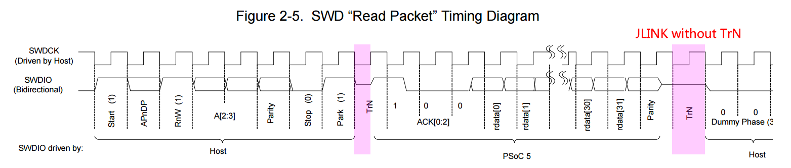
respectively Figure 2-4. SWD “Write Packet” Timing Diagram

a.) Host Write Operation:
Host sends data on the SWDIO line on falling edge of SWDCK and
PSoC 5 reads that data on the next SWDCK rising edge
(for example, 8-bit header data, Write data(wdata[31:0]), Dummy phase (3'b000))
b.) Host Read Operation:
PSoC 5 sends data on the SWDIO line on the rising edge of SWDCK
and the host should read that data on the next SWDCK falling edge
(Ex: ACK data (ACK[2:0]) z z
c.) The host should not drive the SWDIO line during TrN phase.
During first TrN phase (½ cycle duration) of SWD packet,
PSoC 5 starts driving the ACK data on the SWDIO line on the rising edge of SWDCK.
The host should read the data on the subsequent falling edge of SWDCK.
The second TrN phase is 1.5 SWDCK clock cycles.
Both PSoC 5 and the Host will not drive the line during the entire second TrN phase (indicated as ‘z’).
Host should start sending the Write data (wdata) on the next falling edge of SWDCK after second TrN phase.
d.) “DUMMY” phase is three SWD clock cycles with SWDIO line low.
This DUMMY phase is not part of SWD protocol.
The three extra clocks with SWDIO low are required for the Test Controller in PSoC 5
to complete the Read/Write operation when the SWDCK clock is not free-running.
For a reliable implementation, include three IDLE clock cycles with SWDIO low for each packet.
According to the SWD protocol, the host can generate any number of SWD clock cycles between two packets with SWDIO low.
a.) Host Write Operation:
Host sends data on the SWDIO line on falling edge of SWDCK
and PSoC 5 reads that data on the next SWDCK rising edge
(for example, 8-bit header data, dummy phase (3'b000))
b.) Host Read Operation:
PSoC 5 sends data on the SWDIO line on rising edge of SWDCK
and the host should read that data on the next SWDCK falling edge
(for example, ACK data (ACK[2:0], Read data (rdata[31:0]))
c.) The host should not drive the SWDIO line during TrN phase.
During first TrN phase (½ cycle duration) of SWD packet,
PSoC 5 starts driving the ACK data on the SWDIO line on the rising edge of SWDCK.
The host should read the data on the subsequent falling edge of SWDCK.
The second TrN phase is 1.5 SWDCK clock cycles. JLINK use 0.5 SWDCK clock cycles, then enter DUMMY phase.
Both PSoC 5 and the host will not drive the line during the entire second TrN phase (indicated as ‘z’).
Host should start sending the Dummy phase (3'b000) on the next falling edge of SWDCK after second TrN phase.
d.) “DUMMY” phase is three SWD clock cycles with SWDIO line low.
This phase is not part of the SWD protocol.
The three extra clocks with SWDIO low are required for the Test Controller in PSoC 5
to complete the Read/Write operation when the SWDCK clock is not free-running.
For a reliable implementation, include three IDLE clock cycles with SWDIO low for each packet.
According to the SWD protocol, the host can generate any number of SWD clock cycles between two packets with SWDIO low.
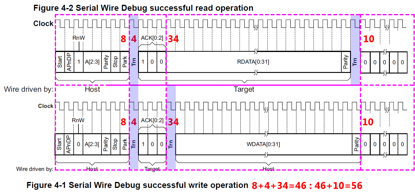
A complete data transfer requires 46 clocks (not including the optional three dummy clock cycles in Figure 2-4 and Figure 2-5).
Each data transfer consists of three phases:
Packet request – External host programmer issues a request to the PSoC 5 device.
Acknowledge response – PSoC 5 sends an acknowledgement to the host.
Data – Data is valid only when a packet request is followed by a valid (OK) acknowledge response.
The data transfer is either:
PSoC 5 to host, following a read request – RDATA
Host to PSoC 5, following a write request – WDATA
In Figure 2-4 and Figure 2-5, the following sequence occurs:
1. The start bit initiates a transfer; it is always logic ‘1’.
2. The APnDP bit determines whether the transfer is an AP access, ‘1’, or a DP access, ‘0’.
3. The next bit is RnW, which is ‘1’ for a read from the PSoC 5 device or ‘0’ for a write to the PSoC 5 device.
4. The ADDR bits (A[3:2]) are register select bits for the access port or debug port.
See Table 2-2 for address bit definitions.
5. The parity bit has the parity of APnDP, RnW, and ADDR. This is an even parity bit.
If the number of logical 1s in these bits is odd, then parity must be ‘1’, otherwise it is ‘0’.
If the parity bit is not correct, the header is ignored by the target device; there is no ACK response.
For the host implementation, the programming operation should be stopped and tried again by doing a device reset.
6. The stop bit is always logic ‘0’.
7. The park bit is always logic ‘1’ and should be driven high by the host.
8. The ACK bits are the device-to-host response. Possible values are shown in Table 2-1.
Note that the ACK in the current SWD transfer reflects the status of the previous transfer.
OK ACK means the previous packet is successful.
WAIT response indicates that the previous packet transaction is not yet complete.
For a Fault operation, the programming operation should be aborted immediately.
- a. For a WAIT response, if it is a read transaction, the host should ignore the data read in the data phase.
PSoC 5 does not drive the line and the host must not check the parity bit.b. For a WAIT response, if it is a write transaction, the data phase is ignored by the PSoC 5 device.
But the host must still send the data to be written from an implementation standpoint.
The parity data corresponding to the data should also be sent by the host.c. For a WAIT response, it means that the PSoC 5 device is processing the previous transaction.
The host can try for a maximum of four continuous WAIT responses to see if an OK response is received,
failing which, it can abort the programming operation and try again.d. For a FAULT response, the programming operation should be aborted and retried by doing a device reset.
9. The data phase includes a parity bit (even parity, similar to the packet request phase).
- a. For a read data packet, if the host detects a parity error,
then it must abort the programming operation and restart. - b. For a write data packet, if the PSoC 5 detects a parity error in the data packet sent by the host,
it generates a FAULT ACK response in the next packet.
10. Turnaround (TrN) phase:
According to the SWD protocol, the TrN phase is used both by the host and the PSoC 5 device
to change the Drive modes on their respective SWDIO line.
There are two TrN phases in each SWD packet.
During the first TrN phase after packet request, PSoC 5 drives the ACK data on the SWDIO line on the rising edge of SWDCK in TrN phase.
This ensures that the host can read the ACK data on the next falling edge.
Thus, the first TrN cycle is only for half cycle duration, as shown in Figure 2-4 and Figure 2-5.
The location of the second TrN phase is different for read and write packets.
The second TrN phase of the SWD packet is one-and-a-half cycle long.
Neither the host nor PSoC 5 should drive SWDIO line during both the TrN phases as indicated by ‘z’ in Figure 2-4 and Figure 2-5.
11. The address, ACK, and read and write data are always transmitted least significant bit (lsb) first.
12. At the end of each SWD packet in Figure 2-4 and Figure 2-5, there is a “DUMMY” phase,
which is three SWD clock cycles with SWDIO line held low.
This DUMMY phase is not part of the SWD protocol.
The three extra clocks with SWDIO low are required for the Test Controller in PSoC 5
to complete the Read/Write operation when the SWDCK clock is not free-running.
For a reliable implementation, include three IDLE clock cycles with SWDIO low for each packet.
According to the SWD protocol, the host can generate any number of SWD clock cycles
between two packets with SWDIO low.
Note The SWD interface can be reset anytime during programming by clocking 51 or more cycles with SWDIO high.
To return to the idle state, SWDIO must be clocked low for three or more cycles. < ADIV5 said, at least 8 cycles >
The host programmer can begin a new SWD packet transaction from the idle state.
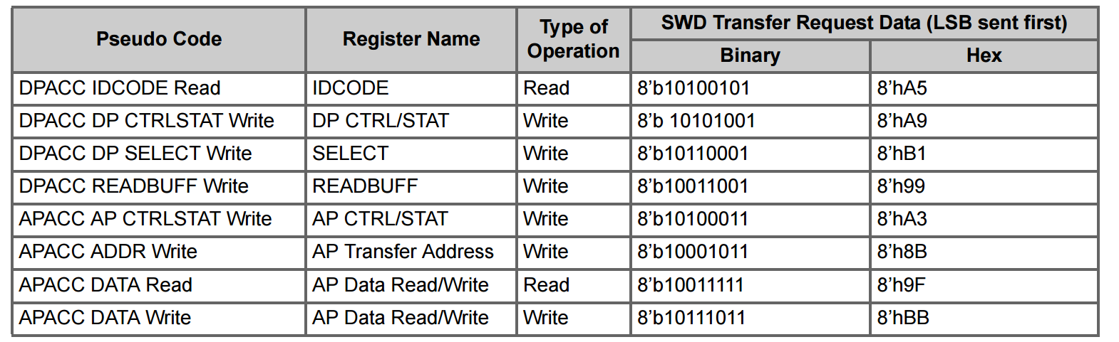
Register Access Using SWD Interface
To access the registers using the SWD interface, in the 8-bit transfer request packet,
set the APnDP bit and select the corresponding ADDR bits, as shown in Table 2-2.
Table 2-3 shows the 8-bit transfer request packet to access the DP and AP registers for read or write operation.
The 8-bit transfer request data in Table 2-3 is transmitted least significant bit first.
The ‘Start’ bit is the least significant bit (LSb) and the ‘Park’ bit is the most significant bit (MSb) in Table 2-3.
Use Table 2-3 and vectors given in SWD Vectors for Programming chapter on page 31 to implement PSoC 5 programming.
Table 2-3. SWD Transfer Request Data Packet for Test Controller DPACC and APACC Register Access
Switching to SWD Interface
PSoC 5 supports programming only through the SWD interface.
It does not support programming through the Joint Test Action Group (JTAG) interface.
But it is necessary to send a JTAG-to-SWD switching sequence on SWDIO, SWDCK lines to program through the SWD interface.
This switching is required in “Step 2: Configure Target Device” on page 21.
The PSoC 5 architecture warrants the switching sequence to SWD interface due to the following reason.
After acquiring the PSoC 5 device, access to the Debug and Access Port (DAP) must be done
by setting the ‘d_tst_acc’ bit in the Test Controller register ‘TC.TST_CR4’.
The Test Controller automatically switches from SWD to JTAG the first time ‘d_tst_acc’ bit
is set, because the DAP always resets to JTAG the first time.
JTAG to SWD switching must be done once during programming as a result of this condition.
But this switching from SWD to JTAG does not happen for subsequent setting of ‘d_tst_acc’ bit while programming.
This is because the DAP remembers its last configuration from that point (until the device is reset by XRES).
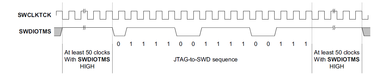

JTAG to SWD Switching
To switch DAP from JTAG to SWD operation, the sequence is as follows:
1. Send 51 or more SWDCK cycles with SWDIO HIGH.
This ensures that the current interface is in its reset state.
The JTAG interface only detects the 16-bit JTAGto-SWD sequence starting from the Test-Logic-Reset state.
2. Send the 16-bit JTAG-to-SWD select sequence on SWDIO.
The 16-bit JTAG-to-SWD select sequence is 0b0111_1001_1110_0111, most-significant bit (MSB) first.
This can be represented as either:
a. 0x79E7 transmitted most-significant bit (MSb) first
b. 0xE79E transmitted least-significant bit (LSb) first.
3. Send 51 or more SWDCK cycles with SWDIO HIGH.
This ensures that if DAP is already in SWD operation before sending the select sequence,
the SWD interface enters line reset state.
4. Send three or more SWDCK cycles with SWDIO low.
This ensures that the SWD line is in the idle state before starting a new SWD packet transaction.
5. Send the DPACC IDCODE READ SWD read packet as given in Table 2-3.
There is no need to process the Device ID returned by the PSoC 5 device for this read packet.
Ignore the Device ID returned by PSoC 5 in this step.
Serial Wire Debug (SWD) Interface -- PSoc5的更多相关文章
- Programming Internal Flash Over the Serial Wire Debug <SWD> Interface -- EFM32
1 Debug Interface Overview 1.1 Serial Wire Debug Serial Wire Debug (SWD) is a two-wire protocol for ...
- SW-DP (Serial Wire Debug Port) Analyzer plugin for the Saleae Logic
SW-DP (Serial Wire Debug Port) Analyzer plugin for the Saleae Logic The SW-DP protocol is described ...
- Implementation of Serial Wire JTAG flash programming in ARM Cortex M3 Processors
Implementation of Serial Wire JTAG flash programming in ARM Cortex M3 Processors The goal of the pro ...
- Introduction to Cortex Serial Wire Debugging
Serial Wire Debug (SWD) provides a debug port for severely pin limited packages, often the case for ...
- Serial Wire Debugging the STM32 via the Bus Pirate
Serial Wire Debugging the STM32 via the Bus Pirate 2 October 2010 Step 1 - The Bus Pirate Step 2 - D ...
- Serial Wire Viewer (SWV)
Being able to display values for counters, sensors and other debugging information is an important p ...
- ARM Cortex Design Considerations for Debug
JTAG was the traditional mechanism for debug connections for ARM7/9 parts, but with the Cortex-M fam ...
- SWD Connect/Transfer Source Code
Serial Wire Debug interface The Serial Wire Debug protocol operates with a synchronous serial interf ...
- swddude -- A SWD programmer for ARM Cortex microcontrollers.
Introducing swddude I love the ARM Cortex-M series of microcontrollers. The sheer computational po ...
随机推荐
- expect 交互 之双引号较长变量
交互双引号较长变量 #!/bin/bash RemoteUser=xuesong12 Ip=192.168.1.2 RemotePasswd=xuesong Cmd="/bin/echo ...
- 01:MFC应用程序编程
一 MFC的发展 VC 1.0->VC 5.0->VC 6.0->VC2008 SP1)->VS2010 二 MFC基础 1 MFC 微软基础类库 采用类的方式,将Win32 ...
- 洛谷 P3320: bzoj 3991: LOJ 2182: [SDOI2015]寻宝游戏
题目传送门:LOJ #2182. 题意简述: 一棵 \(n\) 个节点的树,边有边权. 每个点可能是关键点,每次操作改变一个点是否是关键点. 求所有关键点形成的极小联通子树的边权和的两倍. 题解: 有 ...
- mysql学习------权限机制
MySQL服务器通过MySQL权限表来控制用户对数据库的访问,MySQL权限表存放在mysql数据库里,由mysql_install_db脚本初始化.这些MySQL权限表分别user,db,table ...
- Linux中断(interrupt)子系统之三:中断流控处理层【转】
转自:http://blog.csdn.net/droidphone/article/details/7489756 1. 中断流控层简介 早期的内核版本中,几乎所有的中断都是由__do_IRQ函数 ...
- linux修改文件打开最大数(ulimit命令)
解除 Linux 系统的最大进程数和最大文件打开数限制:vi /etc/security/limits.conf# 添加如下的行* soft noproc 65536 * hard noproc 65 ...
- 安装Scrapy遇到的坑
安装过程怕是要吐血,架梯子等等结果被setuptools的版本给坑了. 参考网址: http://blog.csdn.net/YHYR_YCY/article/details/78876148 htt ...
- mysql及linux发行版下载源
MySQL国内镜像资源 搜狐开源镜像站:http://mirrors.sohu.com/ 国内开源镜像站点汇总 http://segmentfault.com/a/1190000000375848 ...
- scrapy入门二(分页抓取文章入库)
分页抓取博客园新闻,先从列表里分析下一页按钮 相关代码: # -*- coding: utf-8 -*- import scrapy from cnblogs.items import Article ...
- Android Service总结06 之AIDL
Android Service总结06 之AIDL 版本 版本说明 发布时间 发布人 V1.0 初始版本 2013-04-03 Skywang 1 AIDL介绍 AIDL,即And ...