dda的fpga实现(转载)
The general approach using DDAs will be to simulate a system of first-order differential equations, which can be nonlinear. Analog computers use operational amplifiers to do mathematical integration. We will use digital summers and registers. For any set of differential equations with state variables v1 to vm:
dv1/dt = f1(t,v1,v2,v3,...vm)
dv2/dt = f2(t,v1,v2,v3,...vm)
dv3/dt = f3(t,v1,v2,v3,...vm)
...dvm/dt = fm(...)
We will build the following circuitry to perform an Euler integration approximation to these equations in the form
v1(n+1) = v1(n) + dt*(f1(t,v1(n),v2(n),v3(n),...vm(n))
v2(n+1) = v2(n) + dt*(f2(t,v1(n),v2(n),v3(n),...vm(n))
v3(n+1) = v3(n) + dt*(f3(t,v1(n),v2(n),v3(n),...vm(n))
...
vm(n+1) = vm(n) + dt*(fm(...))
Where the variable values at time step n are updated to form the values at time step n+1. Each equation will require one integrator. The multiply may be replaced by a shift-right if dt is chosen to be a power of two. Most of the design complexity will be in calculating F(t,V(n)). 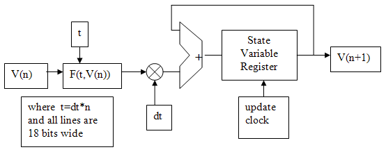
We also need a number representation. I chose 18-bit 2's complement with the binary point between bits 15 and 16 (with bit zero being the least significant). Bit 17 is the sign bit. The number range is thus -2.0 to +1.999985. This range fits well with the Audio codec which requires 16-bit 2's complement for output to the DAC. Conversion from the 18-bit to 16-bit just requires truncating the least significant two bits ([1:0]). A few numbers are shown in the table below. Note that the underscore character in the hexidecimal form is allowed in verilog to improve readability.
|
Decimal number
|
18-bit 2's comp |
|
1.0
|
18'h1_0000
|
|
0.5
|
18'h0_8000
|
|
0.25
|
18'h0_4000
|
|
0
|
18'h0_0000
|
|
-0.25
|
18'h3_c000
|
|
-0.5
|
18'h3_8000
|
|
-1.0
|
18'h3_0000
|
|
-1.5
|
18'h2_8000
|
|
-2.0
|
18'h2_0000
|
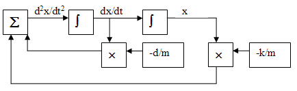
Second order system (damped spring-mass oscillator):
As an example, consider the linear, second-order differential equation resulting from a damped spring-mass system:
d2x/dt2 = -k/m*x-d/m*(dx/dt)
where k is the spring constant, d the damping coefficient, m the mass, and x the displacement. We will simulate this by converting the second-order system into a coupled first-order system. If we let v1=x and v2=dx/dt then the second order equation is equivalent to
dv1/dt = v2
dv2/dt = -k/m*v1-d/m*v2
These equations can be solved by wiring together two integrators, two multipliers and an adder as shown below. In the past this would have been done by using operational amplifiers to compute each mathematical operation. Each integrator must be supplied with an initial condition.
Converting this diagram to Verilog, the top-level module verilog code defines the 18-bit, signed, state variables and a clock divider variable (count). The clocked section resets and updates the state variables. The combinatorial statements compute the Euler approximation to the F(t,V(n)). The separate multiply module ensures that the multiplies will be instantiated as hardware multipliers. The Audio_DAC_ADC module was modifed to allow either ADC-to-DAC passthru or to connect the computation output to the DAC, depending on the position of SW17. SW17 up connects the computation.
/state variables

reg signed [17:0] v1, v2 ;

wire signed [17:0] v1new, v2new ;

//signed mult output

wire signed [17:0] v1xK_M, v2xD_M ;

// the clock divider

reg [4:0] count;

//Update state variables of simulation of spring- mass

	always @ (posedge CLOCK_50)

	begin

		count <= count + 1;

		if (KEY[3]==0) //reset

		begin

			v1 <= 32'h10000 ; //

			v2 <= 32'h00000 ;

			//count <= 0;

		end

		else if (count==0)

		begin

			v1 <= v1new ;

			v2 <= v2new ;

		end

	end

	// Compute new F(t,v) with dt = 2>>9

	// v1(n+1) = v1(n) + dt*v2(n)

	assign v1new = v1 + (v2>>>9);

	// v2(n+1) = v2(n) + dt*(-k/m*v1(n) - d/m*v2(n))

	signed_mult K_M(v1xK_M, v1, 18'h10000);

	signed_mult D_M(v2xD_M, v2, 18'h00800);

	assign v2new = v2 - ((v1xK_M + v2xD_M)>>>9);

module signed_mult (out, a, b);

	output 		[17:0]	out;

	input 	signed	[17:0] 	a;

	input 	signed	[17:0] 	b;

	wire	signed	[17:0]	out;

	wire 	signed	[35:0]	mult_out;

	assign mult_out = a * b;

	assign out = {mult_out[35], mult_out[32:16]};

endmodule
Time scaling the solution requires consideration of the value of dt and the update rate (CLOCK_50/(clock divider)) of the state variables. As shown in the code, the clock divider variable (count) is 5-bits wide, so it will overflow and cause an update every 32 CLOCK_50 cycles. If the time step, dt=2-9, then 29 steps must equal one time unit. 29 steps at an update rate of 5*107/32 yields a time unit of 0.328 mSec. A k/m=1 implies a period of 6.28 time units per cycle, so one cycle in this case would be 2.06 mSec. corresponding to 486 Hz.
If the calculation is scaled in time to be in the audio range, then the audio DAC may be used to watch waveforms on an oscilloscope. For the damped spring-mass oscillator with a k/m=1, d/m=1/16, dt=2-8, and a clock rate of 5*108/64 I got the figure below. The top trace is v1 and the bottom is v2. The frequency computed from the time scaling considerations is 486 Hz, while the measured was 475 Hz. Reducing dt to dt=2-9 (see paragraph above) and the clock divider to 32 made the measured frequency 486, matching the computed value. The better match with smaller dt illustrates that the integration is approximate. 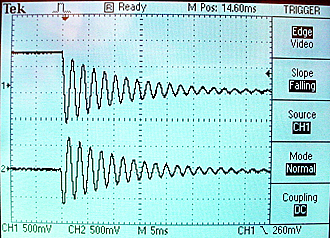
The whole project is zipped here. The design consumed 2% of the logic resources of the FPGA, 1% of the memory, and 4 out of 70 9-bit multipliers. You could threfore expect to put up to 50 integrators and 35 multipilers in a bigger design.
dda的fpga实现(转载)的更多相关文章
- 优化基于FPGA的深度卷积神经网络的加速器设计
英文论文链接:http://cadlab.cs.ucla.edu/~cong/slides/fpga2015_chen.pdf 翻译:卜居 转载请注明出处:http://blog.csdn.net/k ...
- 【转载】FPGA算法映射要点
近期一直在学习利用FPGA完成算法的定点运算,转载些相关的博客方面回顾查找.本博文原文链接为:https://blog.csdn.net/u013989284/article/details/7899 ...
- FPGA功耗那些事儿(转载)
在项目设计初期,基于硬件电源模块的设计考虑,对FPGA设计中的功耗估计是必不可少的.笔者经历过一个项目,整个系统的功耗达到了100w,而单片FPGA的功耗估计得到为20w左右,有点过高了,功耗过高则会 ...
- FPGA静态时序分析——IO口时序(Input Delay /output Delay)(转载)
转载地址:http://www.cnblogs.com/linjie-swust/archive/2012/03/01/FPGA.html 1.1 概述 在高速系统中FPGA时序约束不止包括内部时钟 ...
- [转载]克服FPGA I/O引脚分配挑战--xilinx系列
转载走,放到自己的分类中好了 原文地址:I/O引脚分配挑战--xilinx系列">克服FPGA I/O引脚分配挑战--xilinx系列作者:方槍槍 http://www.eefocus ...
- 【转载】FPGA功耗的那些事儿
在项目设计初期,基于硬件电源模块的设计考虑,对FPGA设计中的功耗估计是必不可少的. 笔者经历过一个项目,整个系统的功耗达到了100w,而单片FPGA的功耗估计得到为20w左右, 有点过高了,功耗过高 ...
- 【转载】FPGA静态时序分析——IO口时序
转自:http://www.cnblogs.com/linjie-swust/archive/2012/03/01/FPGA.html 1.1 概述 在高速系统中FPGA时序约束不止包括内部时钟约束 ...
- 【转载】如何在FPGA设计环境中添加加时序约束
转自:http://bbs.ednchina.com/BLOG_ARTICLE_198929.HTM 如何在FPGA设计环境中加时序约束 在给FPGA做逻辑综合和布局布线时,需要在工具中设定时序 ...
- FPGA设计思想与技巧(转载)
题记:这个笔记不是特权同学自己整理的,特权同学只是对这个笔记做了一下完善,也忘了是从那DOWNLOAD来的,首先对整理者表示感谢.这些知识点确实都很实用,这些设计思想或者也可以说是经验吧,是很值得每一 ...
随机推荐
- Java String类为什么不可变?
原文地址:# Why String is immutable in Java? 众所周知,String类在Java中是不可变的.不可变类简单地说是实例不可修改的类.对于一个实例创建后,其初始化的时候所 ...
- Runtime.getRuntime.exec();
杀死Chrome浏览器进程 private static void closeAllChrome() throws IOException{ Runtime.getRuntime().exec(&qu ...
- weblogic 12c重置console密码
su - oracle cd /u02/weblogic/user_projects/domains/base_domain source bin/setDomainEnv.sh cd /u02/ ...
- 1-16-1 LVM管理和ssm存储管理器使用&磁盘配额
大纲: 1-1- LVM逻辑卷的管理 1-2- SSM管理工具的使用 1-3- 磁盘配额技巧 ====================================== 问题描述: 当我们需要在一个 ...
- JAVA执行带参数的SQL语句
转自 http://www.cnblogs.com/raymond19840709/archive/2008/05/12/1192948.html
- poj-2342-简单树形dp
Anniversary party Time Limit: 1000MS Memory Limit: 65536K Total Submissions: 10388 Accepted: 594 ...
- Opencv+pycharm+anaconda配置
最简便的方法,没有之一 首先下载annconda:(不要从官网下,还要FQ,还要慢) https://mirrors.tuna.tsinghua.edu.cn/anaconda/archive/ 请注 ...
- IOS-APP前需要考虑的几件事
做一个 App 前需要考虑的几件事 来源:Limboy's HQ 链接:http://t.cn/R5sEDMJ 随着工具链的完善,语言的升级以及各种优质教程的涌现,做一个 App 的成本也越来越低了. ...
- 拒绝了对对象 'sp_OACreate' (数据库 'mssqlsystemresource',架构 'sys')的 EXECUTE 权限。
执行一个存储过程, 由于里面使用到了一些 --创建对象 EXEC sp_OACreate 'VBScript.RegExp', @objRegex OUT --设置属性 EXEC sp_OASe ...
- SVM之解决线性不可分
SVM之问题形式化 SVM之对偶问题 SVM之核函数 >>>SVM之解决线性不可分 写在SVM之前——凸优化与对偶问题 上一篇SVM之核函数介绍了通过计算样本核函数,实际上将样本映射 ...