JTAG – A technical overview and Timing
This document provides you with interesting background information about the technology that underpins XJTAG. You do not need to know any of this however to be able to use the XJTAG development system as XJTAG tests are developed in a high-level programming language that does not require any knowledge of the detailed working of JTAG.
Introduction
Advances in silicon design such as increasing device density and, more recently, BGA packaging have reduced the efficacy of traditional testing methods.
In order to overcome these problems, some of the world's leading silicon manufacturers combined to form the Joint Test Action Group. The findings and recommendations of this group were used as the basis for the Institute of Electrical and Electronic Engineers (IEEE) standard 1149.1: Standard Test Access Port and Boundary Scan Architecture. This standard has retained its link to the group and is commonly know by the acronym JTAG.
Boundary Scan
The main advantage offered by utilising boundary scan technology is the ability to set and read the values on pins without direct physical access.

The process of boundary scan can be most easily understood with reference to the schematic diagram shown in figure 1.
All the signals between the device's core logic and the 'pins' are intercepted by a serial scan path known as the Boundary Scan Register (BSR). In normal operation these boundary scan cells are invisible. However, in test mode the cells can be used to set and/or read values: in external mode these will be the values of the 'pins'; in 'internal' mode these will the values of the core logic.
Interface Signals
The JTAG interface, collectively known as a Test Access Port, or TAP, uses the following signals to support the operation of boundary scan.
- TCK (Test Clock) – this signal synchronizes the internal state machine operations.
- TMS (Test Mode Select) – this signal is sampled at the rising edge of TCK to determine the next state.
- TDI (Test Data In) – this signal represents the data shifted into the device's test or programming logic. It is sampled at the rising edge of TCK when the internal state machine is in the correct state.
- TDO (Test Data Out) – this signal represents the data shifted out of the device's test or programming logic and is valid on the falling edge of TCK when the internal state machine is in the correct state.
- TRST (Test Reset) – this is an optional pin which, when available, can reset the TAP controller's state machine.
Registers
There are two types of registers associated with boundary scan. Each compliant device has one instruction register and two or more data registers.
Instruction Register – the instruction register holds the current instruction. Its content is used by the TAP controller to decide what to do with signals that are received. Most commonly, the content of the instruction register will define to which of the data registers signals should be passed.
Data Registers – there are three primary data registers, the Boundary Scan Register (BSR), the BYPASS register and the IDCODES register. Other data registers may be present, but they are not required as part of the JTAG standard.
- BSR – this is the main testing data register. It is used to move data to and from the I/O pins of a device.
- BYPASS – this is a single-bit register that passes information from TDI to TDO. It allows other devices in a circuit to be tested with minimal overhead.
- IDCODES – this register contains the ID code and revision number for the device. This information allows the device to be linked to its Boundary Scan Description Language (BSDL) file. The file contains details of the Boundary Scan configuration for the device.
Test Access Port (TAP) Controller
The TAP controller, a state machine whose transitions are controlled by the TMS signal, controls the behaviour of the JTAG system. Figure 2, below, shows the state-transition diagram.
All states have two exits, so all transitions can be controlled by the single TMS signal sampled on TCK. The two main paths allow for setting or retrieving information from either a data register or the instruction register of the device. The data register operated on (e.g. BSR, IDCODES, BYPASS) depends on the value loaded into the instruction register.
For more detail on each state, refer to the IEEE 1149.1 Standard JTAG document.
Boundary Scan Instructions
The IEEE 1149.1 standard defines a set of instructions that must be available for a device to be considered compliant. These instructions are:
- BYPASS – this instruction causes the TDI and TDO lines to be connected via a single-bit pass-through register (the BYPASS register). This instruction allows the testing of other devices in the JTAG chain without any unnecessary overhead.
- EXTEST – this instruction causes the TDI and TDO to be connected to the Boundary Scan Register (BSR). The device's pin states are sampled with the 'capture dr' JTAG state and new values are shifted into the BSR with the 'shift dr' state; these values are then applied to the pins of the device using the 'update dr' state.
- SAMPLE/PRELOAD – this instruction causes the TDI and TDO to be connected to the BSR. However, the device is left in its normal functional mode. During this instruction, the BSR can be accessed by a data scan operation to take a sample of the functional data entering and leaving the device. The instruction is also used to preload test data into the BSR prior to loading an EXTEST instruction.
Other commonly available instructions include:
- IDCODE – this instruction causes the TDI and TDO to be connected to the IDCODE register.
- INTEST – this instruction causes the TDI and TDO lines to be connected to the Boundary Scan Register (BSR). While the EXTEST instruction allows the user to set and read pin states, the INTEST instruction relates to the core-logic signals of a device.
JTAG TAP
TAP状态机只和TCK、TMS有关。一般在TCK的下降沿更新TMS、TDI的电平,在TCK的上升沿采样TDO的电平,这样保证建立保持时间是符合要求的,数据是稳定的。
TAP状态切换图

可以看到一般情况下TMS为高的时候会切换状态,TMS为低的时候是保持,而Test-Logic-Reset是在TMS为高的时候保持。
这么设计的目的是,如果不知道当前的状态,那么拉高TMS,持续5个TCK时钟就一定可以跳转到Test-Logic-Reset状态(仔细看看状态跳转图)。
以下只是为了说明在各个状态下,DR收到TCK后的行为,并不是实际的代码。 IR的实现是类似的。
Select-DR-Scan
//verilog

always@(posedge TCK)

begin

    if ((tap == SELECT_DR_SCAN) && !TMS)

        addr_reg <= ADDR_DR;

    else

        addr_reg <= addr_reg;

end
Capture-DR
//verilog

always@(posedge TCK)

begin

    if (tap == CAPTURE_DR)

        r_dr <= odata_dr;

    else

        r_dr <= r_dr;

end
可以看到当从Capture-DR跳转到Shift-DR后,TDO已经是有效的了,但是TDI并没有移入。
只有在Shift-DR的状态给出TCK上升沿才能移入TDI数据。
Shift-DR
//verilog

always@(posedge TCK)

begin

    if (tap == SHIFT_DR)

        r_dr <= {r_dr, TDI};

    else

        r_dr <= r_dr;

end
需要注意的是最后从Shift-DR跳转到Exit1-DR的时候DR寄存器还是会移入一位TDI, 所以在处理的时候需要特别的注意。
一般如果DR有N位,那么前N-1位保持TMS为0, 在最后一次需要把TMS置1。
我最开始的时候就是没有注意这部分,导致移位总错。
Pause-DR
这个用途看起来没有用,其实还是可以好好用的,比如用SPI实现JTAG的时序,
如果那个SPI只能配置成8或16位,那么移位数据的时候一定是8的倍数的TCK上升沿,
在Pause-DR状态停留几次就可以保证不会有错误的状态跳转了。
Update-DR
//verilog

always@(posedge TCK)

begin

    if ((tap == UPDATE_DR)

        io <= dr;

    else

        io <= io;

end

Here we can see what things look like from a logic analyzer.
(when the JTAG clock is clocking things at 10MHz, and the Logic Analyzer is sampling at 200MHz).

The way this works is that the above state diagram is followed, decoding the TMS (mode select) pin.
The TDI and TDO pins are used to shift data in and out of the JTAG registers,
(JTAG Instruction Registers, and JTAG data registers).
For example, 13 TCK rising edges occur while TMS is zero.
This will loop things in the RUN-TEST/IDLE state.
Then it clocks in two ones.
This will move things to the Select-IR-Scan state.
A zero moves it to the capture-IR, and 5 more clocks,
shift the TDI into the JTAG Instruction register (in time, it shifts 1100100 into the IR).
The Instruction register is five bits wide and accommodates up to 32 boundary-scan instructions.
The Instruction register holds both public and private instructions.
The JTAG standard requires some of the public instructions;
other public instructions are optional.
Private instructions are reserved for the manufacturer’s use.
Since the IR is only 5 bits long, it keeps 00100..
The JTAG Instruction Register (IR) is just a pointer into which JTAG data register data should be passed.

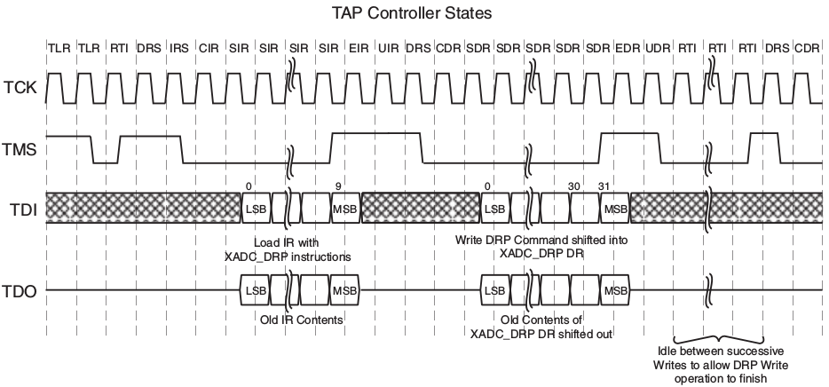
JTAG Timing
The timing of the JTAG signals is shown below.
The TDO pin remains in the high impedance state except during a shift-DR or shift-IR controller state.
In the shift-DR and shift-IR controller states,
TDO is updated on the falling edge of TCK by Target.
Sampled on the rising edge of TCK by Host.
TMS and TDI are sampled on the rising edge of TCK by Target.
Updated on the falling edge or TCK by Host.


The test logic consists of a Boundary-Scan register and other building blocks.
The test logic is accessed through what is commonly referred to as the Test Access Port or TAP.
The TAP consists of 6 pins
| Name | Type | Description |
|---|---|---|
| TCK | Input | JTAG Clock |
| TDO | Output | JTAG Serial Data Out |
| TDI | Input | JTAG Serial Data In |
| TMS | Input | JTAG Mode Select |
| TRST | Input | JTAG Reset |
| EMU | Output | Emulation Output |
The first step of understanding JTAG is understanding the validity of the data,
or when is the data clocked into/out of the JTAG port by the test device, or emulator.
If we use the Blackfin processor as an example - the datasheet indicates something like:

Timing Requirements
| symbol | Description | Specification |
|---|---|---|
| tTCK | TCK Period | min 20 ns |
| tSTAP | TDI, TMS Setup Before TCK High | min 4 ns |
| tHTAP | TDI, TMS Hold After TCK High | min 4 ns |
| tTRSTW | TRST Pulse Width (Measured in TCK cycles) | min 4 TCK cycles |
Switching Characteristics
| symbol | Description | Specification |
|---|---|---|
| tDTDO | TDO Delay from TCK Low |
max 10 ns |
The JTAG specification section 6.3.1.c indicates “Where a dedicated reset pin (TRST*)
is provided to allow initialization of the TAP controller,
initialization shall occur asynchronously when the TRST* input changes to the low logic level.”,
this is not true on the Blackfin, where a min TRST pulse width of 4 TCLK cycles is necessary.
JTAG Interfaces
The TPS65950 Joint Test Action Group (JTAG) test access port (TAP) controller handles standard IEEE JTAG interfaces.
The JTAG/TAP module provides a JTAG interface according to IEEE Standard 1149.1a.
This interface uses the four I/O pins TMS, TCK, TDI, and TDO. The TMS, TCK, and TDI inputs contain a pullup device,
which makes their state high when they are not driven.
The output TDO is a 3-state output, which is high impedance except when data are shifted between TDI and TDO:
- TCK is the test clock signal.
- TMS is the test mode select signal.
- TDI is the scan path input.
- TDO is the scan path output.
The JTAG operations are controlled by a state-machine that follows the IEEE Standard 1149.1a state diagram.
The input timing requirements are given by considering a rising or falling edge of 7 ns. The capacitive load is 35 pF.

Table 4-11 JTAG Interface Timing Requirements
| Notation | Parameter | Min | Max | Unit | |
|---|---|---|---|---|---|
| Clock | |||||
| JL1 | tc(TCK) | Cycle time, JTAG.TCK period | 30 | ns | |
| JL2 | tw(TCK) | Pulse duration, JTAG.TCK high or low(1) | 0.48*P | 0.52*P | ns |
| Read Timing | |||||
| JL3 | tsu(TDIV-TCKH) | Setup time, JTAG.TDI valid before JTAG.TCK high | 8 | ns | |
| JL4 | th(TDIV-TCKH) | Hold time, JTAG.TDI valid after JTAG.TCK high | 5 | ns | |
| JL5 | tsu(TMSV-TCKH) | Setup time, JTAG.TMS valid before JTAG.TCK high | 8 | ns | |
| JL6 | th(TMSV-TCKH) | Hold time, JTAG.TMS valid after JTAG.TCK high | 5 | ns | |
Table 4-12 JTAG Interface Switching Characteristics
| Notation | Parameter | Min | Max | Unit | |
|---|---|---|---|---|---|
| Write Timing | |||||
| JL7 | td(TCK-TDOV)) | Delay time, JTAG, TCK active edge to JTAG.TDO valid | 0 | 14 | ns |
JTAG Electrical Data and Timing, Timing Requirements for JTAG

| NO. | OPP100 | OPP50 | UNIT | ||||
|---|---|---|---|---|---|---|---|
| MIN | MAX | MIN | MAX | ||||
| 1 | tc(TCK) | Cycle time, TCK | 81.5 | 104.5 | ns | ||
| 1a | tw(TCKH) | Pulse duration, TCK high (40% of tc) | 32.6 | 41.8 | ns | ||
| 1b | tw(TCKL) | Pulse duration, TCK low (40% of tc) | 32.6 | 41.8 | ns | ||
| 3 | tsu(TDI-TCKH) | Input setup time, TDI valid to TCK high | 3 | 3 | ns | ||
| tsu(TMS-TCKH) | Input setup time, TMS valid to TCK high | 3 | 3 | ns | |||
| 4 | th(TCKH-TDI) | Input hold time, TDI valid from TCK high | 8.05 | 8.05 | ns | ||
| th(TCKH-TMS) | Input hold time, TMS valid from TCK high | 8.05 | 8.05 | ns | |||
| NO. | PARAMETER | OPP100 | OPP50 | UNIT | |||
|---|---|---|---|---|---|---|---|
| MIN | MAX | MIN | MAX | ||||
| 2 | td(TCKL-TDO) | Delay time, TCK low to TDO valid | 3 | 27.6 | 4 | 36.8 | ns |
JTAG Scan Interface Timing

| No. | Parameter | Min | MAX | Unit | |
|---|---|---|---|---|---|
| fTCK | TCK frequency (at HCLKmax) | 12 | MHz | ||
| fRTCK | RTCK frequency (at TCKmax and HCLKmax) | 10 | MHz | ||
| 1 | td(TCK -RTCK) | Delay time, TCK to RTCK | 24 | ns | |
| 2 | tsu(TDI/TMS - RTCKr) | Setup time, TDI, TMS before RTCK rise (RTCKr) | 21 | ns | |
| 3 | th(RTCKr -TDI/TMS) | Hold time, TDI, TMS after RTCKr | 0 | ns | |
| 4 | th(RTCKr -TDO) | Hold time, TDO after RTCKf | 0 | ns | |
| 5 | td(TCKf -TDO) | Delay time, TDO valid after RTCK fall (RTCKf) | 10 | ns | |
JTAG – A technical overview and Timing的更多相关文章
- 9. Technical Overview 技术概述
9.1 Runtime Environment 运行环境 Spring Security 3.0需要Java 5.0运行时环境或更高版本.由于Spring Security的目标是以独立的方式运行,所 ...
- Technical analysis of client identification mechanisms
http://www.chromium.org/Home/chromium-security/client-identification-mechanisms Chromium > Chro ...
- 如何在 arm 官网上找到合适的手册
http://infocenter.arm.com/help/advanced/help.jsp 在这里输入合适的版号即可 这样就可以不用去 CSDN 了 100000_0000_00_EN - AR ...
- 翻译:微软style的并行计算
Parallel Microsoft-Style By Andrew Binstock, July 20, 2011 Note:主要是自动翻译,俺做了小量修改 1 Comment The actor ...
- STM32F4xx -- Cortex M4
STM32F4xx official page: http://www.st.com/internet/mcu/subclass/1521.jspIntroductionFPU - Floating ...
- (转) [it-ebooks]电子书列表
[it-ebooks]电子书列表 [2014]: Learning Objective-C by Developing iPhone Games || Leverage Xcode and Obj ...
- 基于Linux的WebSphere性能调优与故障诊断
一.关于was数据源等问题的配置 (1)关于was数据源连接池的最大.最小配置多大合适?怎样去计算? (2)关于JVM的配置,64位系统,64位WAS,最值小和最大配置多大最优?怎样去计算? (3)应 ...
- BizTalk 开发系列(三十九) BizTalk Server 2009技术概览
BizTalk Server 2009已经发布一段时间了,之前Beta版发布的时候也写过一篇文章<BizTalk Server 2009 Beta初体验>, 当时比较了2006 R2与20 ...
- Mac OS X 背后的故事
Mac OS X 背后的故事 作者: 王越 来源: <程序员> 发布时间: 2013-01-22 10:55 阅读: 25840 次 推荐: 49 原文链接 [收藏] ...
随机推荐
- iOS8 UICollectionView横向滑动demo
在iOS8中,scrollView和加载在它上面的点击事件会有冲突,所以做一个横向滑动的界面最好的选择就是UICollectionView. 这个效果可以用苹果公司提供的官方demo修改而来,下载地址 ...
- expect 交互 之双引号较长变量
交互双引号较长变量 #!/bin/bash RemoteUser=xuesong12 Ip=192.168.1.2 RemotePasswd=xuesong Cmd="/bin/echo ...
- size属性
size 属性 size 属性规定输入字段的尺寸(以字符计): <form action=""> First name:<br> <input typ ...
- 使用 scm-manager 搭建 git/svn 代码管理仓库(二)
主要介绍scm的配置. 1.配置为在Windows服务中启动scm-manager的启动方式有多种,可以在DOS(即命令行CMD模式)中启动,也可以在Windows服务中启动. 下面我们采用Windo ...
- Vue's Demo
*.vue=<template> </template>+<style></style>+<script></script> s ...
- PHP中冒号、endif、endwhile、endfor使用介绍
我们经常在wordpress一类博客程序的模板里面看到很多奇怪的PHP语法,比如: 复制代码代码如下: <?php if(empty($GET_['a'])): ?> <font c ...
- hdu 4348 To the moon (主席树)
版权声明:本文为博主原创文章,未经博主允许不得转载. hdu 4348 题意: 一个长度为n的数组,4种操作 : (1)C l r d:区间[l,r]中的数都加1,同时当前的时间戳加1 . (2)Q ...
- history命令追查登录的用户和时间
Linux查看History记录加时间,这个对于系统管理员还是很有帮助的,原因不解释,你懂得!ora11g$ history | more 1 rlwrap sqlplus / as sy ...
- linux:查询软件是否安装以及删除
参考网址:http://blog.sina.com.cn/s/blog_6d59e57d0102x21u.html 查询java是否安装 rpm -qa |grep java 批量卸载所有带有Java ...
- 【linux】shell中命令替换$(cmd)和符号`cmd`
来源:https://zhidao.baidu.com/question/485498670.html 作用: $(cmd)和`cmd`的作用是相同的,在执行一条命令时,会先将其中的 ``,或者是$( ...