RAM-Based Shift Register (ALTSHIFT_TAPS) IP Core-实现3X3像素阵列存储
最近想要实现CNN的FPGA加速处理,首先明确在CNN计算的过程中,因为卷积运算是最耗时间的,因此只要将卷积运算在FPGA上并行实现,即可完成部分运算的加速
那么对于卷积的FPGA实现首先要考虑的是卷积子模板具体如何实现,我们在matlab或者c实现比如3X3的子模板的时候,只要用一个数组即可将模板的数据存储起来,而在FPGA的话有以下三种方法:
- 用2个或3个RAM存储3X3像素阵列
- 用2个或3个FIFO存储3X3像素阵列
- 用shift_RAM移位存储3X3像素阵列
而shift_RAM好像就是为了阵列的实现量身定做的一般。
shift_RAM的配置参数主要有以下几个:

手册中可以参考理解的一个非常形象的图如下:

进一步的进行单独一个IP核的仿真后得到:
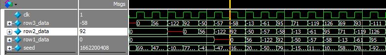
其中上述参数设置分别为8,2,3,上述仿真图中,相当于把一个矩阵A通过移位寄存的方法通过row3_data送入到RAM,然后分三行输出,在游标所示处就可以开始输出3X3矩阵
0,56,-122
92,50,-57
-58,-13,-61
以下部分是加入了对视频信号处理控制后的代码实现过程:
/*-----------------------------------------------------------------------

CONFIDENTIAL IN CONFIDENCE

This confidential and proprietary software may be only used as authorized

by a licensing agreement from CrazyBingo (Thereturnofbingo).

In the event of publication, the following notice is applicable:

Copyright (C) 2011-20xx CrazyBingo Corporation

The entire notice above must be reproduced on all authorized copies.

Author                :        CrazyBingo

Technology blogs     :         http://blog.chinaaet.com/crazybingo

Email Address         :         thereturnofbingo@gmail.com

Filename            :        VIP_Matrix_Generate_3X3_8Bit.v

Data                :        2014-03-19

Description            :        Generate 8Bit 3X3 Matrix for Video Image Processor.

                            Give up the 1th and 2th row edge data caculate for simple process

                            Give up the 1th and 2th point of 1 line for simple process

Modification History    :

Data            By            Version            Change Description

=========================================================================

13/05/26        CrazyBingo    1.0                Original

14/03/16        CrazyBingo    2.0                Modification

-*/

`timescale 1ns/1ns

module VIP_Matrix_Generate_3X3_8Bit

#(

    parameter    [:]    IMG_HDISP = 'd640,    //640*480

    parameter    [:]    IMG_VDISP = 'd480

)

(

    //global clock

    input                clk,                  //cmos video pixel clock

    input                rst_n,                //global reset

    //Image data prepred to be processd

    input                per_frame_vsync,    //Prepared Image data vsync valid signal

    input                per_frame_href,        //Prepared Image data href vaild  signal

    input                per_frame_clken,    //Prepared Image data output/capture enable clock

    input        [:]    per_img_Y,            //Prepared Image brightness input

    //Image data has been processd

    output                matrix_frame_vsync,    //Prepared Image data vsync valid signal

    output                matrix_frame_href,    //Prepared Image data href vaild  signal

    output                matrix_frame_clken,    //Prepared Image data output/capture enable clock

    output    reg    [:]    matrix_p11, matrix_p12, matrix_p13,    //3X3 Matrix output

    output    reg    [:]    matrix_p21, matrix_p22, matrix_p23,

    output    reg    [:]    matrix_p31, matrix_p32, matrix_p33

);

//Generate 3*3 matrix

//--------------------------------------------------------------------------

//--------------------------------------------------------------------------

//--------------------------------------------------------------------------

//sync row3_data with per_frame_clken & row1_data & raw2_data

wire    [:]    row1_data;    //frame data of the 1th row

wire    [:]    row2_data;    //frame data of the 2th row

reg    [:]    row3_data;    //frame data of the 3th row

always@(posedge clk or negedge rst_n)

begin

    if(!rst_n)

        row3_data <= ;

    else

        begin

        if(per_frame_clken)

            row3_data <= per_img_Y;

        else

            row3_data <= row3_data;

        end

end

//---------------------------------------

//module of shift ram for raw data

wire    shift_clk_en = per_frame_clken;

Line_Shift_RAM_8Bit

#(

    .RAM_Length    (IMG_HDISP)

)

u_Line_Shift_RAM_8Bit

(

    .clock        (clk),

    .clken        (shift_clk_en),    //pixel enable clock

//    .aclr        (1'b0),

    .shiftin    (row3_data),    //Current data input

    .taps0x        (row2_data),    //Last row data

    .taps1x        (row1_data),    //Up a row data

    .shiftout    ()

);

//------------------------------------------

//lag 2 clocks signal sync  因为数据存储耗费了一个时钟,因此3*3阵列读取使能和时钟要偏移一个时钟

reg    [:]    per_frame_vsync_r;

reg    [:]    per_frame_href_r;

reg    [:]    per_frame_clken_r;

always@(posedge clk or negedge rst_n)

begin

    if(!rst_n)

        begin

        per_frame_vsync_r <= ;

        per_frame_href_r <= ;

        per_frame_clken_r <= ;

        end

    else

        begin

        per_frame_vsync_r     <=     {per_frame_vsync_r[],     per_frame_vsync};

        per_frame_href_r     <=     {per_frame_href_r[],     per_frame_href};

        per_frame_clken_r     <=     {per_frame_clken_r[],     per_frame_clken};

        end

end

//Give up the 1th and 2th row edge data caculate for simple process

//Give up the 1th and 2th point of 1 line for simple process

wire    read_frame_href        =    per_frame_href_r[];    //RAM read href sync signal

wire    read_frame_clken    =    per_frame_clken_r[];    //RAM read enable

//将存储RAM以及阵列生成两个步骤需要的时钟都去掉

assign    matrix_frame_vsync     =     per_frame_vsync_r[];

assign    matrix_frame_href     =     per_frame_href_r[];

assign    matrix_frame_clken     =     per_frame_clken_r[];

//----------------------------------------------------------------------------

//----------------------------------------------------------------------------

/******************************************************************************

                    ----------    Convert Matrix    ----------

                [ P31 -> P32 -> P33 -> ]    --->    [ P11 P12 P13 ]

                [ P21 -> P22 -> P23 -> ]    --->    [ P21 P22 P23 ]

                [ P11 -> P12 -> P11 -> ]    --->    [ P31 P32 P33 ]

******************************************************************************/

//---------------------------------------------------------------------------

//---------------------------------------------------

/***********************************************

    (1) Read data from Shift_RAM

    (2) Caculate the Sobel

    (3) Steady data after Sobel generate

************************************************/

//wire    [23:0]    matrix_row1 = {matrix_p11, matrix_p12, matrix_p13};    //Just for test

//wire    [23:0]    matrix_row2 = {matrix_p21, matrix_p22, matrix_p23};

//wire    [23:0]    matrix_row3 = {matrix_p31, matrix_p32, matrix_p33};

always@(posedge clk or negedge rst_n)

begin

    if(!rst_n)

        begin

        {matrix_p11, matrix_p12, matrix_p13} <= 'h0;

        {matrix_p21, matrix_p22, matrix_p23} <= 'h0;

        {matrix_p31, matrix_p32, matrix_p33} <= 'h0;

        end

    else if(read_frame_href)

        begin

        if(read_frame_clken)    //Shift_RAM data read clock enable

            begin

            {matrix_p11, matrix_p12, matrix_p13} <= {matrix_p12, matrix_p13, row1_data};    //1th shift input

            {matrix_p21, matrix_p22, matrix_p23} <= {matrix_p22, matrix_p23, row2_data};    //2th shift input

            {matrix_p31, matrix_p32, matrix_p33} <= {matrix_p32, matrix_p33, row3_data};    //3th shift input

            end

        else

            begin

            {matrix_p11, matrix_p12, matrix_p13} <= {matrix_p11, matrix_p12, matrix_p13};

            {matrix_p21, matrix_p22, matrix_p23} <= {matrix_p21, matrix_p22, matrix_p23};

            {matrix_p31, matrix_p32, matrix_p33} <= {matrix_p31, matrix_p32, matrix_p33};

            end

        end

    else

        begin

        {matrix_p11, matrix_p12, matrix_p13} <= 'h0;

        {matrix_p21, matrix_p22, matrix_p23} <= 'h0;

        {matrix_p31, matrix_p32, matrix_p33} <= 'h0;

        end

end

endmodule

//注意这里得到的每一行得第一第二的像素都没有用到,而且最后一行的像素没有被运算。
RAM-Based Shift Register (ALTSHIFT_TAPS) IP Core-实现3X3像素阵列存储的更多相关文章
- 阅读 RAM-Based Shift Register(ALTSHIFT_TAPS) IP Core User Guide
阅读 RAM-Based Shift Register(ALTSHIFT_TAPS) IP Core User Guide 说明:本文档自带测试工程: DE_ALTSHIFT_TAPS.zip 1.支 ...
- Modelsim独立仿真Vivado Clocking Wizard IP Core
工欲善其事,必先利其器.在使用Vivado自带的仿真软件仿真的时候,相对于更优秀的仿真工具Modelsim,效率低了很多,为了更高效的开发,我尝试着用Vivado级联Modelsim仿真,但是级联后还 ...
- 在EDK里面添加ISE IP core的方法
(1)在ISE下,使用core generator,可以得到xilinx的IP的*.v和*.ngc 文件,将这两个文件拷贝出来: (2)在EDK下使用“Create or Import Periphe ...
- 使用xilinx ip core FIFO First- World First-Through (FWFT)模式的注意事项
也许很多人知道xilinx ip core 中的fifo可以配成standard 模式和FWFT模式,并知道两者的区别是:standard模式下,当rd为高时,fifo会延时一个时钟输出数据(时序逻辑 ...
- IP Core 分类
IP(Intelligent Property)核是具有知识产权核的集成电路芯核总称,是经过反复验证过的.具有特定功能的宏模块,与芯片制造工艺无关,可以移植到不同的半导体工艺中.到了SOC阶段,IP核 ...
- H.265 Video Encoder IP Core
复制: 开源H.265硬件视频编码器H.265 Video Encoder IP Core是开源的H.265硬件视频编码器,实现了H.265(或叫HEVC)的大部分功能. 它由复旦大学专用集成电路与系 ...
- Vivado 2017封装自定义IP Core
使用Vivado2017.3自定义IP Core.通常情况下,我们做设计采用模块化设计,对于已经设计好的一部分模块功能,就可以直接拿来调用,IP Core就是这样来的,一般来说我们看不到IP Core ...
- Xilinx 7系列例化MIG IP core DDR3读写
昨晚找了一下,发现DDR3读写在工程上多是通过例化MIG,调用生成IPcore的HDL Functional Model.我说嘛,自己哪能写出那么繁琐的,不过DDR读写数据可以用到状态机,后期再添砖加 ...
- Shift Register(Using Submodule)
/*************************************************** / Shift Register module by Submodule / Progra ...
随机推荐
- Maven - Eclipse例子
版权所有,未经授权,禁止转载 章节 Maven – 简介 Maven – 工作原理 Maven – Repository(存储库) Maven – pom.xml 文件 Maven – 依赖管理 Ma ...
- 谈谈我近一个半月的dp练习
前请提示:https://www.cnblogs.com/caiyishuai/p/9047991.html 配合这篇文章食用风味更佳哦! 首先十分感谢henry_y提供的50道dp练习,链接在这 ...
- win10编译jpeglib
jpeglib看名字都大概知道和图像格式jpg或jpeg有关了,是一个常用的图像处理软件都会依赖的开源库. 首先去官网下载jpeglib的源码,直接取这里下载:http://www.ijg.org/f ...
- VS2019企业版产品密钥
Visual Studio 2019 Enterprise产品密钥(激活码) BF8Y8-GN2QH-T84XB-QVY3B-RC4DF
- 寒假day17-本周计划
完善人才的数据挖掘模块 结合当下疫情完成人才动态模块 修正人才标签部分 优化界面
- Eclipse上传Git远程仓库,并且增加Maven Dependencies
前言: 遇见问题了,公司一台电脑,家里一台电脑,当有项目在进行的时候,又不想把电脑背来背去的,就像一个人玩单机,这个时候GIT就可以帮你解决这个问题.当GIT准备就绪的时候,新的问题来了git下载下载 ...
- JavaScript—面向对象 贪吃蛇_2 游戏对象
游戏对象 function Game(map) { this.map = map; this.food = new Food(this.map) this.snake = new Snake(this ...
- c#连接sql server数据库字符串
第一种方式 Data Source=数据库地址;Initial Catalog=数据库名称;User Id=数据库登录名;Password=数据库密码;[Integrated Security=SSP ...
- 基于迅为-i.MX6Q开发板制作镜像方法
在“/home/imx6”目录(在前面编译 android 系统的时候新建过这个目录,如果没有可以自己新建一个)下,使用命令“mkdir minilinux/”新建 minilinux 目录,使用命令 ...
- javaweb学习——session和Cookie实现购物车功能
1.创建Book类,实现对图书信息的封装. package cn.it.sessionDemo.example1; import java.io.Serializable; /** * 该类实现对图书 ...