Down to the TLP: How PCI express devices talk (Part I)
http://xillybus.com/tutorials/pci-express-tlp-pcie-primer-tutorial-guide-1
Down to the TLP: How PCI express devices talk (Part I)
Foreword
While I was writing the Xillybus IP core for PCI express, I quickly found out that it’s very difficult to start off: Online resources as well as the official spec bombards you with gory details about the nuts and bolts, but says much less about what the machine is supposed to do. So once I made the effort to figure that out for myself, I decided to write this little guide, which will hopefully help others get a softer start. This is based upon the official PCI Express specification 1.1, but applies very well to later versions. There is no substitute to reading the original spec, though. The name of the game if to get the details right, so that the device works properly in environments that are not at hand for testing.
Don’t pick on me for not describing the whole picture, or using inaccurate definitions. Being accurate is what the spec is for. All I’m trying to do here is to making it more human readable. I’ve also published a sample TLP sniff dump of a session, which may help understand how the machinery works.
And I rely on other sources to describe form factors, lane counts, data rates and such. For an overview of these, I suggest Wikipedia’s entry on this. I also suggest to read about PCI configuration, in particular the part about enumeration.
So let’s start with some basic insights.
PCI express is not a bus
The first thing to realize about PCI express (PCIe henceforth), is that it’s not PCI-X, or any other PCI version. The previous PCI versions, PCI-X included, are true buses: There are parallel rails of copper physically reaching several slots for peripheral cards. PCIe is more like a network, with each card connected to a network switch through a dedicated set of wires. Exactly like a local Ethernet network, each card has its own physical connection to the switch fabric. The similarity goes further: The communication takes the form of packets transmitted over these dedicated lines, with flow control, error detection and retransmissions. There are no MAC addresses, but we have the card’s physical (“geographic”) position instead to define it, before it’s allocated with high-level means of addressing it (a chunk in the I/O and address space).
As a matter of fact, a minimal (1x) PCIe connection merely consists of four wires for data transmission (two differential pairs in each direction) and another pair of wires to supply the card with a reference clock. That’s it.
On the other hand, the PCIe standard was deliberately made to behave very much like classic PCI. Even though it’s a packet-based network, it’s all about addresses, reads, writes an interrupt.
There’s still the plug-and-play configuration done, and the cards are accessed in terms of reads and writes to address and I/O space, just like before. There are still Vendor/Product IDs, and several mechanisms to mimic old behavior. To make a long story short, the PCIe standard goes a long way to look like good old PCI to an operation system unaware of PCIe.
So PCIe is a packet network faking the traditional PCI bus. Its entire design makes it possible to migrate a PCI device to PCIe without making any change in software, and/or transparently bridge between PCI and PCIe without losing any functionality.
A simple bus transaction
In order to get an understanding of the whole things, let’s see what happens when a PC’s CPU wants to write a 32-bit word to a PCIe peripheral. Several details and possibilities are deliberately left out for sake of simplicity in the description below.
Since it’s a PC, it’s likely that the CPU itself performs a simple write operation on its own bus, and that the memory controller chipset, which is connected to the CPU’s bus, has the direct connection to the PCIe bus. So what happens is that the chipset (which, in PCIe terms functions as a Root Complex) generates a Memory Write packet for transmission over the bus. This packet consists of a header, which is either 3 or 4 32-bit words long (depending on if 32 or 64 bit addressing is used) and one 32-bit word containing the word to be written. This packet simply says “write this data to this address”.
This packet is then transmitted on the chipset’s PCIe port (or one of them, if there are several). The target peripheral may be connected directly to the chipset, or there may be a switch network between them. This way or another, the packet is routed to the peripheral, decoded, and executed by performing the desired write operation.
A closer look
This simplistic view ignores several details. For example, the underlying communications mechanism, which consists of three layers: The Transaction Layer, the Data Link Layer, and the Physical Layer. The description of the packet above was defined as a Transaction Layer Packet (TLP), which relates to PCIe’s uppermost layer.
The Data Link layer is responsible for making sure that every TLP arrives to its destination correctly. It wraps TLPs with its own header and with a Link CRC, so that the TLP’s integrity is assured. An acknowledge-retransmit mechanism makes sure no TLPs are lost on the way. A flow control mechanism makes sure a packet is sent only when the link partner is ready to receive it. All in all, whenever a TLP is handed over to the Data Link Layer for transmission, we can rely on its arrival, even if there is a slight uncertainty regarding the time of arrival. Failing to deliver a TLP is a major malfunction of the bus.
We’ll come back to the Data Link Layer when discussing credits and packet reordering. But to this end, it’s enough to realize that classic bus operations are substituted by transmission of a TLP over the PCIe fabric.
I’d also like to mention that a Memory Write TLP’s data payload may be significantly longer than a single 32-bit word, forming a PCIe write burst. The TLP’s size limits are set at the peripheral’s configuration stage, but typical numbers are a maximum of 128, 256 or 512 bytes per TLP.
And before going on, it’s worth to note that the sender of a Memory Write TLP doesn’t get an indication that the packet has reached its final destination, even less that it has been executed. Even though the Data Link Layer gets a positive acknowledge, that only means that the packet made its way safely to the nearby switch. No end-to-end acknowledgment is ever made, and neither is it really necessary.
A sample write packet
Let’s take the data write case mentioned above, and see the details of the TLP. Suppose that the CPU wrote the value 0x12345678 to the physical address 0xfdaff040 using 32-bit addressing. The packet could then consist of four 32-bit words (4 DWs, Double Words) as follows:
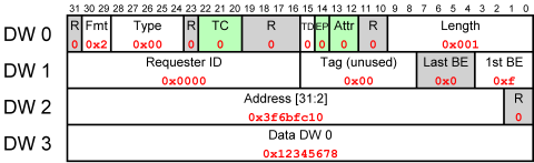
Example of Memory Write Request TLP
So the packet was transmitted as 0x40000001, 0x0000000f, 0xfdaff040, 0x12345678.
Let’s just explain the color coding:
- Gray fields are reserved, which means that the sender has to put zeros there (and the receiver ignore them). Some gray fields are marked “R” which means that the field is always reserved, and some have a name, meaning that the field is reserved because of the nature of this specific packet.
- Green fields are allowed to have nonzero values, but they are rarely used by endpoint peripherals (from what I’ve seen).
- The values of the specific packet are marked in red.
Now let’s briefly explain the valid fields:
- The Fmt field, together with the Type field say this is a Memory Write Request.
- The TD bit is zero, indicating that there is no extra CRC on the TLP data (TLP Digest). This extra CRC has no justification if we trust our hardware not to corrupt the TLPs, since the Link Layer has its own CRC to make sure nothing gets wrong on the way.
- The Length field has the value 0x001, indicating that this TLP has one DW (32-bit word) of data.
- The Requester ID field says that the sender of this packet is known by having ID zero — it’s the Root Complex (the PCIe port closest to the CPU). While mandatory, this field has no practical use in a Write Request, except for reporting back errors.
- The Tag is an unused field in this case. The sender can put anything here, and all other components should ignore it. We shall get a closer look at it later.
- The 1st BE field (1st Double-Word Byte Enable) allows to choose which of the four bytes in the first data DW are valid, and should be written. Set as 0xf in our case, it marks that all four bytes are written to.
- The Last BE field must be zero when Length is unity, since the first DW and the last is the same one.
- The Address field is simply the address to which the first data DW is written. Well, bits 31-2 of this address. Note that the two LSBs of DW 2 in the TLP are zero, so DW 2 actually reads the write address itself. Multiply 0x3f6bfc10 by four, and you get 0xfdaff040.
- And finally, we have one DW of data. This is a good time to mention that PCIe runs big Endian, and Intel processors think little Endian. So if this was a regular PC computer, it was writing 0x78563412 in its software representation.
A Read Request
Now let’s see what happens when the CPU wants to read from a peripheral. Read operations are a bit more tricky, because inevitably there are going to be two packets involved: One TLP from the CPU to the peripheral, asking the latter to perform a read operation, and one TLP going back with the data. In PCIe terms we have a Requester (the CPU in our case) and a Completer (the peripheral).
We’ll assume that the CPU wants a single a single DW (32-bit word) from address 0xfdaff040 (same as before). As before, it’s likely that it initiates a read operation on the bus it shares with its memory controller, which contains the Root Complex, which in turn generates a TLP to be sent over the PCIe bus. It’s a Read Request TLP, which may look like this:
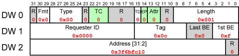
Example of Memory Read Request TLP
So this packet consists of the 3 DWs 0x00000001, 0x00000c0f, 0xfdaff040. It tells the peripheral to read one full DW at address 0xfdaff040, and to return the result to the bus entity whose ID is 0x0000.
It’s strikingly similar to the Write Request example shown above, so I’ll focus on the differences:
- The Fmt/Type fields have changed (actually, only Fmt) to indicate this is a Read Request.
- As before, The Requester ID field says that the sender of this packet has ID zero. It’s the same field as before, but in a Read Request it’s functionally crucial, since it tells the Completer where to send its response. We’ll see more about this ID below.
- The Tag is significant in Read Requests. It’s important to realize that it doesn’t mean anything by itself, but that it has the function of a tracking number: When the Completer responds, it must copy this value to the Completion TLP. This allows the Requester to match Completion answers with its Request. After all, multiple requests from a single device on a bus are allowed. This Tag is set by the Requester for its own needs, and the standard doesn’t require a certain enumeration method, as long as the Tags of all outstanding requests are unique. Despite the 8 bits allocated, only the 5 LSBs are allowed for use, and the rest must be zero by default. This allows for a maximum of 32 outstanding requests between a pair of bus entities. For applications that need it, in-standard extensions may allow as many as 2048.
The Length field indicates that one DW should be read, and the Address field from which address. The two BE fields retain the same meaning and rules as with a Write Request, only they pick which bytes to read rather than which bytes to write.
The considerations for applying read requests are discussed on another tutorial.
The Completion
When the peripheral receives a Read Request TLP, it must respond with some sort of Completion TLP, even if it can’t fulfill the action requested. We’re going to look at a successful case: The peripheral read the chunk of data from its internal resources, and now needs to return the result back to the Requester (the CPU in our case).
The packet could look like this:
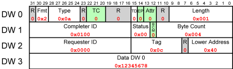
Example of Completion TLP
So the TLP consists of 0x4a000001, 0x01000004, 0x00000c00, 0x12345678. The packets basically says “tell bus entity 0x0000 that the answer to its Request to entity 0x0100, which was tagged 0x0c, is 0x12345678.” The CPU (or actually, the memory controller = Root Complex) can now look up in its internal records what that request was about, and complete the relevant bus cycle. Let’s chop it down to pieces:
- The Fmt field, together with the Type field say this is a Completion packet with data.
- The Length field has the value 0x001, indicating that this TLP has one DW (32-bit word) of data. But wait. Isn’t the Requester supposed to know that anyhow? The answer is that there’s a limit to a TLP’s length, which may be less than the number of DWs requsted. When that happens, several Completion TLPs are sent back. So the Length field says how many DWs are in this specific packet. But that’s a different story.
- And if we’re at it, we have the Byte Count field. In our case of a single-TLP completion, it’s simply the number of valid payload bytes in the packet. Since the 1st DW BE field in the Request was all ones, we have four valid bytes, as stated in the field. Just for general knowledge, the real definition of this field is the number of bytes left for transmission, including those in the current packet. That’s useful in multiple TLP completions, as demonstrated just below.
- Then we have Lower Address field. It’s the 7 least significant bits of the address, from which the first byte in this TLP was read. It’s 0x40 in our case, coming from the lower bits of 0xfdaff040. This field can be useful with multiple TLP completions.
- The Completer ID identifies the sender of this packet, which is 0x1000. I’ll dissect this ID below.
- The Requester ID identifies the receiver of this packet, which is zero ID (Root Complex). If there’s some PCIe switches to route through, this serves as the destination address.
- The Status field is zero, indicating that the Completion was successful. As one can guess, other values indicate different types of rejections.
- The BCM field is always zero, except when a packet origins from a bridge with PCI-X. So it’s zero.
- And finally, we have one DW of data.
By the way, the Completer may return the data sliced up into several packets. The last packet in the completion can then be detected by checking for
Length == ((LowerAddress & 3) + ByteCount + 3) >> 2
and if we happen to restrict ourselves to DW-granularity in our requests, this simply becomes
Length == ByteCount >> 2
So much for these two examples. Now some more general speaking.
Posted and non-Posted operations
If we compare the life cycle of a bus write operation with the one of a read, there’s an evident difference: A write TLP operation is fire-and-forget. Once the packet has been formed and handed over to the Data Link Layer, there’s no need to worry about it anymore. A read operation, on the other hand, requires the Requester to wait for a Completion. Until the Completion packet arrives, the Requester must retain information about what the Request was, and sometimes even hold the CPU’s bus: If the CPU’s bus started a read cycle, it must be held in wait states until the value of the desired read operation is available at the bus’ data lines. This can be a horrible slowdown of the bus, which is rightfully avoided in recent systems.
The terminology for fire-and-forget operations, such as a Memory Write is Posted operations. Such operations consist of a Request only. Naturally, operations that consist of a Request and Completion are called non-Posted operations.
I/O Requests
The PCIe bus supports I/O operations only for the sake of backward compatibility, and strongly recommends not to use I/O TLPs in new designs. One of the reasons is that both read and write requests in I/O space are non-Posted, so the Requester is forced to wait for a completion on write operations as well. Another issue is that I/O operations only take 32-bit addresses, while the PCIe spec endorses 64-bit support in general.
Identification and routing
Since PCIe is essentially a packet network, with the possibility of switches on the way, these switches need to know where to send each TLP. There are three routing methods: By address, by ID and implicit. By address routing is applied for Memory and I/O Requests (read and write). Implicit routing is used only for certain message TLPs, such as broadcasts from Root Complex and messages that always go to the Root Complex. All other TLPs are routed by ID.
The ID is a 16-bit word formed in terms of the well known triplet: Bus number, Device number and Function number. Their meaning is exactly like in legacy PCI buses. The ID is formed as follows:
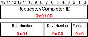
Formation of PCIe ID
If you’re running Linux, I suggest trying the lspci utility with its numerous flags to get friends with the bus structure.
Bus Mastering (DMA)
This issue used to be a bit spooky until PCIe. After all, there’s something intrusive about telling the CPU to step aside from the bus, now I’m running the show.
On PCIe, it’s significantly less exotic. It boils down to the simple notion, that anyone on the bus can send read and write TLPs on the bus, exactly like the Root Complex. This allows the peripheral to access the CPU’s memory directly (DMA) or exchange TLPs with peer peripherals (to the extent that the switching entities support that).
Well, there are two things that need to happen first, as with any PCI device: The peripheral needs to be granted bus mastering by setting the “Bus Master Enable” bit in one of the standard configuration registers. The second thing is that the driver software needs to inform the peripheral about the relevant buffer’s physical address, most probably by writing to a BAR-mapped register.
Interrupts
PCIe supports two kinds of interrupts: Legacy INTx and MSI.
INTx interrupts are supported for the sake of compatibility with legacy software, and also in order to allow bridging between classic PCI buses and PCIe. Since INTx interrupts are level triggered (i.e. the interrupt request is active as long as the physical INTx wire is at low voltage), there’s a TLP packet for saying that the line has been asserted, and another that it has been deasserted. Not only is this a quirky in itself, but the old problems with INTx interrupts retain, such as interrupt sharing and the need for each interrupt handling routine to check who the interrupt is really for.
It was because of these issues, that a new form of interrupt, MSI, was introduced in (conventional) PCI 2.2. The idea was, that since virtually all PCI peripherals have bus master capabilities, why not let the peripheral signal an interrupt by writing to a certain address?
PCIe does exactly the same to generate an MSI: Signaling an interrupt merely consists of sending a TLP over the bus, which is simply a posted Write Request, with a special address, which the host has written into the peripheral’s configuration space during initialization. Any modern operating system (Linux included, of course) can then call the correct interrupt routine, without the need to guess who generated the interrupt. Neither is it really necessary to “clear” the interrupt, if the peripheral doesn’t need the acknowledgment.
Down to the TLP: How PCI express devices talk (Part I)的更多相关文章
- Down to the TLP: How PCI express devices talk (Part II)
http://xillybus.com/tutorials/pci-express-tlp-pcie-primer-tutorial-guide-2 Data Link Layer Packets A ...
- PCI Express(四) - The transaction layer
原文出处:http://www.fpga4fun.com/PCI-Express4.html 感觉没什么好翻译的,都比较简单,主要讲了TLP的帧结构 In the transaction layer, ...
- Ubuntu 16.04 RTL8111/8168/8411 PCI Express Gigabit Ethernet Controller” 不能上网
来源:http://forum.ubuntu.org.cn/viewtopic.php?f=116&t=463646 1.执行如下命令 uname -a sudo lspci -knn sud ...
- [中英对照]How PCI Express Works | PCIe工作原理
How PCI Express Works | PCIe工作原理 PCI Express is a high-speed serial connection that operates more li ...
- PCI Express
1.1课题研究背景 在目前高速发展的计算机平台上,应用软件的开发越来越依赖于硬件平台,尤其是随着大数据.云计算的提出,人们对计算机在各个领域的性能有更高的需求.日常生活中的视频和图像信息包含大量的数据 ...
- 了解PCI Express的Posted传输与Non-Posted传输
0.写在前面 本文首发于公众号[两猿社],后续将在公众号内持续更新~ 其实算下来接触PCIe很久了,但是由于之前换工作,一直没有系统的学习和练手项目,现在新项目买了Synopsys的PCIe IP,总 ...
- PCI Express(六) - Simple transactions
原文地址:http://www.fpga4fun.com/PCI-Express6.html Let's try to control LEDs from the PCI Express bus. X ...
- PCI Express(五) - Xilinx wizard
原文地址:http://www.fpga4fun.com/PCI-Express5.html Xilinx makes using PCI express easy - they provide a ...
- PCI Express(三) - A story of packets, stack and network
原文出处:http://www.fpga4fun.com/PCI-Express3.html Packetized transactions PCI express is a serial bus. ...
随机推荐
- spring3.0注解定时任务配置及说明
spring注解方式的定时任务配置: 第一步:spring配置文件 <?xml version="1.0" encoding="UTF-8"?> & ...
- ASP.NET中的ExecuteNonQuery()方法的用法
下面我将详细讲解在机房收费系统D层中如何对数据库的增加.删除.修改,最后再来总结一下 ExecuteNonQuery(),ExecuteScalar(),ExecuteReader的用法: 一.增.删 ...
- poj2752 Seek the Name, Seek the Fame(next数组的运用)
题目链接:id=2752" style="color:rgb(202,0,0); text-decoration:none; font-family:Arial; font-siz ...
- 这么多的技术,作为一个freshman,什么研究?
科学技术,从哪里学习? 杨问了我几个最近:"如何学习技术?".说实话,其实,我自己只是一个资深兄弟.对于这个答案.这是更难以在本身回答. 可是.既然比师弟们多吃了几年 ...
- 兔子--Fragment与ViewPager要切换滑动效果
效果图: 文件夹结构: 代码分析: MainActivity.java package com.example.myfragment; /** * @author Arthur Lee * @time ...
- 趣味Java算法题(附答案)
[程序1] 题目:古典问题:有一对兔子,从出生后第3个月起每一个月都生一对兔子,小兔子长到第三个月后每一个月又生一对兔子,假如兔子都不死,问每一个月的兔子总数为多少? //这是一个菲波拉契 ...
- ios在SQLite3基本操作
iOS关于sqlite3操作 iPhone中支持通过sqlite3来訪问iPhone本地的数据库. 详细用法例如以下 1:加入开发包libsqlite3.0.dylib 首先是设置项目文件.在项目中加 ...
- HTML<!DOCTYPE> 宣示
在html页面,下面这行代码到底有什么用呢? <!DOCTYPE html PUBLIC "-//W3C//DTD XHTML 1.0 Transitional//EN" & ...
- 用于编译cm-12.0 的 local_manifest.xml文件
将代码保存为 romservice.xml文件 <?xml version="1.0" encoding="UTF-8"?> <manifes ...
- 【BZOJ 1642】 [Usaco2007 Nov]Milking Time 挤奶时间
1642: [Usaco2007 Nov]Milking Time 挤奶时间 Time Limit: 5 Sec Memory Limit: 64 MB Submit: 590 Solved: 3 ...