
推荐 的FPGA设计经验(4) 时钟和寄存器控制架构特性使用
Use Clock and Register-Control Architectural Features
FPGAs provide device-wide clocks and register control signals that can improve performance.
Use Global Clock Network Resources
Altera FPGAs provide device-wide global clock routing resources and dedicated inputs. Use the FPGA’s low-skew, high fan-out dedicated routing where available.
FPGAs offer a number of low-skew global routing resources to distribute high fan-out signals to help withthe implementation of large designs with many clock domains.
Use Global Reset Resources
ASIC designs may use local resets to avoid long routing delays. Take advantage of the device-wide asynchronous reset pin available on most FPGAs to eliminate these problems. This reset signal provides low-skew routing across the device.
The following are three types of resets used in synchronous circuits:
• Synchronous Reset
• Asynchronous Reset
• Synchronized Asynchronous Reset—preferred when designing an FPGA circuit
Use Synchronous Resets
The synchronous reset ensures that the circuit is fully synchronous. You can easily time the circuit with the Quartus Prime TimeQuest analyzer.
Because clocks that are synchronous to each other launch and latch the reset signal, the data arrival and data required times are easily determined for proper slack analysis. The synchronous reset is easier to use with cycle-based simulators.
There are two methods by which a reset signal can reach a register; either by being gated in with the data input, or by using an LAB-wide control signal (synclr).
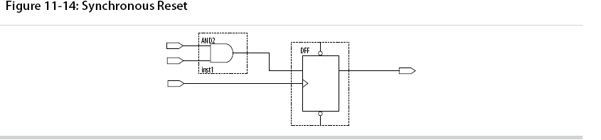
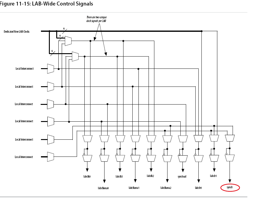
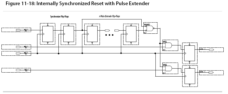
Consider two types of synchronous resets when you examine the timing analysis of synchronous resets—externally synchronized resets and internally synchronized resets.
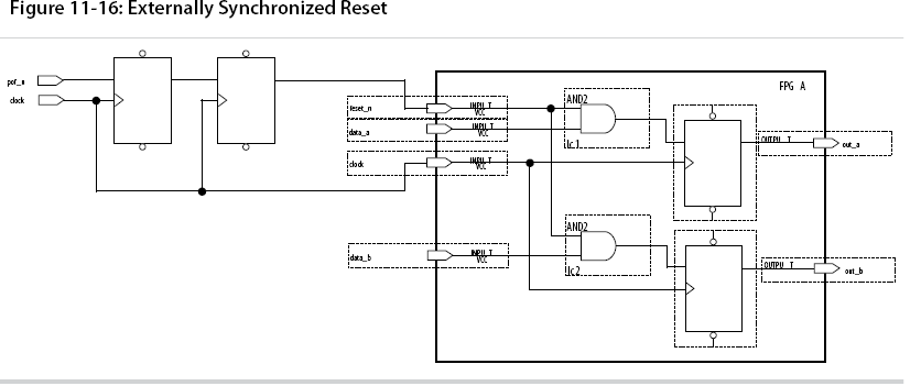
module sync_reset_ext (

input clock,

input reset_n,

input data_a,

input data_b,

output out_a,

output out_b

);

reg reg1, reg2;

assign out_a = reg1;

assign out_b = reg2;

always @ (posedge clock)

begin

if (!reset_n)

begin

reg1 <= ’b0;

reg2 <= ’b0;

end

else

begin

reg1 <= data_a;

reg2 <= data_b;

end

end

endmodule // sync_reset_ext
verilog code for externally synchronized reset
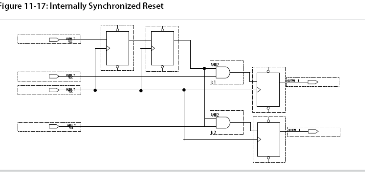
module sync_reset (

input clock,

input reset_n,

input data_a,

input data_b,

output out_a,

output out_b

);

reg reg1, reg2;

reg reg3, reg4;

assign out_a = reg1;

assign out_b = reg2;

assign rst_n = reg4;

always @ (posedge clock)

begin

if (!rst_n)

begin

reg1 <= ’bo;

reg2 <= ’b0;

end

else

begin

reg1 <= data_a;

reg2 <= data_b;

end

end

always @ (posedge clock)

begin

reg3 <= reset_n;

reg4 <= reg3;

end

endmodule // sync_reset
verilog code for internally synchronized reset
In some cases, you might want to increase the noise immunity further and reject any asynchronous input reset that is less than n periods wide to debounce an asynchronous input reset.
Using Asynchronous Resets
Asynchronous resets are the most common form of reset in circuit designs, as well as the easiest to implement.
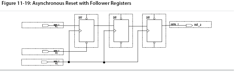
However, when the reset is deasserted and does not pass the recovery (μtSU) or removal (μtH) time check (the TimeQuest analyzer recovery and removal analysis checks both times), the edge is said to have fallen into the metastability zone.
To avoid this, add a few follower registers after the register with the asynchronous reset and use the output of these registers in the
design.
module async_reset (

input clock,

input reset_n,

input data_a,

output out_a,

);

reg reg1, reg2, reg3;

assign out_a = reg3;

always @ (posedge clock, negedge reset_n)

begin

if (!reset_n)

reg1 <= ’b0;

else

reg1 <= data_a;

end

always @ (posedge clock)

begin

reg2 <= reg1;

reg3 <= reg2;

end

endmodule // async_reset
verilog code of asychronous reset with follower register
The asynchronous reset is susceptible to noise, and a noisy asynchronous reset can cause a spurious reset. You must ensure that the asynchronous reset is debounced and filtered. You can easily enter into a reset asynchronously, but releasing a reset asynchronously can lead to potential problems (also referred to as “reset removal”) with metastability, including the hazards of
unwanted situations with synchronous circuits involving feedback.
Use Synchronized Asynchronous Reset
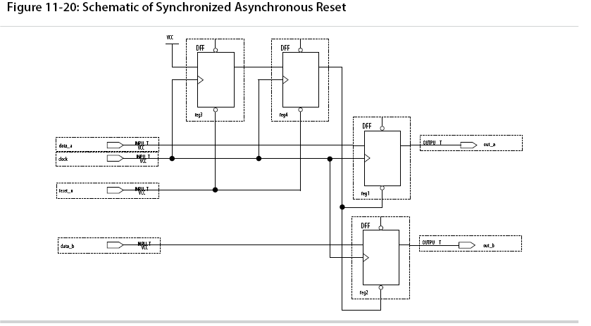
To avoid potential problems associated with purely synchronous resets and purely asynchronous resets, you can use synchronized asynchronous resets. Synchronized asynchronous resets combine the advantages of synchronous and asynchronous resets.
This takes effect almost instantaneously, and ensures that no data path for speed is involved, and that the circuit is synchronous for timing analysis and is resistant to noise.
module sync_async_reset (

input clock,

input reset_n,

input data_a,

input data_b,

output out_a,

output out_b

);

reg reg1, reg2;

reg reg3, reg4;

assign out_a = reg1;

assign out_b = reg2;

assign rst_n = reg4;

always @ (posedge clock, negedge reset_n)

begin

if (!reset_n)

begin

reg3 <= ’b0;

reg4 <= ’b0;

end

else

begin

reg3 <= ’b1;

reg4 <= reg3;

end

end

always @ (posedge clock, negedge rst_n)

begin

if (!rst_n)

begin

reg1 <= ’b0;

reg2 <= ;b0;

end

else

begin

reg1 <= data_a;

reg2 <= data_b;

end

end

endmodule // sync_async_reset
verilog code for synchronized asynchronous reset
To minimize the metastability effect between the two synchronization registers, and to increase
the MTBF, the registers should be located as close as possible in the device to minimize routing delay. If possible, locate the registers in the same logic array block (LAB).
Avoid Asynchronous Register Control Signals
Avoid using an asynchronous load signal if the design target device architecture does not include registers with dedicated circuitry for asynchronous loads. Also, avoid using both asynchronous clear and preset if the architecture provides only one of these control signals.
When the target device does not directly support the signals, the synthesis or placement and routing software must use combinational logic to implement the same functionality. In addition, if you use signals in a priority other than the inherent priority in the device architecture, combinational logic may be required to implement the necessary control signals. Combinational logic is less efficient and can cause glitches and other problems; it is best to avoid these implementations.
Implementing Embedded RAM
Altera’s dedicated memory architecture offers many advanced features that you can enable with Altera provided IP cores. Use synchronous memory blocks for your design, so that the blocks can be mapped directly into the device dedicated memory blocks.
In many synthesis tools, you can specify that the read-during-write behavior is not important to your design; if, for example, you never read and write from the same address in the same clock cycle. For
Quartus Prime integrated synthesis, add the synthesis attribute ramstyle=”no_rw_check” to allow the software to choose the read-during-write behavior of a RAM, rather than using the read-during-write
behavior specified in your HDL code. Using this type of attribute prevents the synthesis tool from using extra logic to implement the memory block and, in some cases, can allow memory inference when it
would otherwise be impossible.
推荐 的FPGA设计经验(4) 时钟和寄存器控制架构特性使用的更多相关文章
- 推荐 的FPGA设计经验(2)-时钟策略优化
Optimizing Clocking Schemes Avoid using internally generated clocks (other than PLLs) wherever possi ...
- 推荐 的FPGA设计经验(3) 物理实现和时间闭环优化
Optimizing Physical Implementation and Timing Closure Planning Physical Implementation When planning ...
- 推荐 的FPGA设计经验(1)组合逻辑优化
主要内容摘自Quartus prime Recommended Design Practices For optimal performance, reliability, and faster ti ...
- 影响FPGA设计中时钟因素的探讨。。。转
http://www.fpga.com.cn/advance/skill/speed.htm http://www.fpga.com.cn/advance/skill/design_skill3.ht ...
- FPGA分频与倍频的简单总结(涉及自己设计,调用时钟IP核,调用MMCM原语模块)
原理介绍 1.分频 FPGA设计中时钟分频是重要的基础知识,对于分频通常是利用计数器来实现想要的时钟频率,由此可知分频后的频率周期更大.一般而言实现偶数系数的分频在程序设计上较为容易,而奇数分频则相对 ...
- FPGA设计思想与技巧(转载)
题记:这个笔记不是特权同学自己整理的,特权同学只是对这个笔记做了一下完善,也忘了是从那DOWNLOAD来的,首先对整理者表示感谢.这些知识点确实都很实用,这些设计思想或者也可以说是经验吧,是很值得每一 ...
- 【设计经验】2、ISE中ChipScope使用教程
一.软件与硬件平台 软件平台: 操作系统:Windows 8.1 开发套件:ISE14.7 硬件平台: FPGA型号:XC6SLX45-CSG324 二.ChipScope介绍 ChipScope是X ...
- 【转】 FPGA设计的四种常用思想与技巧
本文讨论的四种常用FPGA/CPLD设计思想与技巧:乒乓操作.串并转换.流水线操作.数据接口同步化,都是FPGA/CPLD逻辑设计的内在规律的体现,合理地采用这些设计思想能在FPGA/CPLD设计工作 ...
- FPGA 设计流程,延迟,时间
FPGA 设计流程,延迟,时间 流程:每个时钟周期可以传输的数据比特. 延迟:从输入到时钟周期的输出数据需要经验. 时间:两个元件之间的最大延迟,最高时钟速度. 1 採用流水线能够提高 流量: 比如计 ...
随机推荐
- sql语句的group by 与 inner join
一.理解group by和聚合函数 先来看下表1,表名为test: 表1 执行如下SQL语句: 1 2 SELECT name FROM test GROUP BY name 你应该很容易知道运行的结 ...
- 显示锁(ReentranLock)
1. Lock接口:定义了一组抽象的加锁操作,提供了一种无条件的.可轮询的.定时的以及可中断的锁获取操作,所有的加锁和解锁的方法都是显示的. 2. ReentrantLock锁:实现了Lock接口,并 ...
- 代码注释模板(把内容保存为xml文件,导入eclipse中即可)
<?xml version="1.0" encoding="UTF-8" standalone="no"?><templa ...
- 快速搭建一个SSM框架demo
我之所以写一个快速搭建的demo,主要想做一些容器的demo,所以为了方便大家,所以一切从简,简单的3层架构 先用mysql的ddl,后期不上oracle的ddl ; -- ------------- ...
- 14、SpringBoot-CRUD错误处理机制(1)
一.springboot默认的处理机制 1.浏览器返回一个错误的页面 默认处理错误:返回一个错误的页面: 包括错误类型.时间...... 2.其他客户端访问 默认响应一个json数据 原理: 错误 ...
- 在Windows 7和10上显示上次登录帐户信息
组策略: 计算机配置->管理模板->Windows组件->Windows登录选项 现在注销并重新登录以查看会发生什么. 在进入桌面之前,用户必须确认该消息 注册表: 打开: &quo ...
- maven学习利用Profile构建不同环境的部署包
项目开发好以后,通常要在多个环境部署,象我们公司多达5种环境:本机环境(local).(开发小组内自测的)开发环境(dev).(提供给测试团队的)测试环境(test).预发布环境(pre).正式生产环 ...
- 关于swing界面label和button的动态设置文字
在引入发送验证码功能后,想让button的文本动态变化,发现如下方法并不能做到: int limitSec=10; while(limitSec>0){ sendyzhm.setEnabled( ...
- File常见操作函数
String Name = File.getName(); //获得文件或文件夹的名称: String parentPath = File.getParent(); //获得文件或文件夹的父目录 ...
- 如何在github上实现预览
这个问题在网络上有很多答案,但是真正能解决的寥寥无几!接下来我就来尝试一下网络上疯传的几种方法.准备好了吗?我要开车了!!! PS:以下实验上传到github的demo采取导入本地css,js和网络上 ...