
推荐 的FPGA设计经验(2)-时钟策略优化
Optimizing Clocking Schemes
Avoid using internally generated clocks (other than PLLs) wherever possible because they can cause functional and timing problems in the design.
Use clock setting assignments on any derived or internal clocks to specify their relationship to the base clock.
Use global device-wide, low-skew dedicated routing for all internally-generated clocks, instead of
routing clocks on regular routing lines.
Avoid data transfers between different clocks wherever possible. If you require a data transfer between different clocks, use FIFO circuitry.
You can use the clock uncertainty features in the Quartus Prime software to compensate for the variable delays between clock domains. Consider setting a clock setup uncertainty and clock hold uncertainty value of 10% to 15% of the clock delay.
Register Combinational Logic Outputs
If you use the output from combinational logic as a clock signal or as an asynchronous reset signal, you can expect to see glitches in your design. In a synchronous design, glitches on data inputs of registers are normal events that have no consequences. However, a glitch or a spike on the clock input (or an asynchronous input) to a register can have significant consequences.
To avoid these problems, you should always register the output of combinational logic before you use it as a clock signal.

Avoid Asyncrhonous Clock Division
Using dedicated PLL circuitry can help you to avoid many of the problems that can be introduced by asynchronous clock division logic.
When you must use logic to divide a master clock, always use synchronous counters or state machines. Additionally, create your design so that registers always directly generate divided clock signals, and route the clock on global clock resources. To avoid glitches, do not decode the outputs of a counter or a state machine to generate clock signals.
Avoid Ripple Counters
Ripple counters use cascaded registers, in which the output pin of one register feeds the clock pin of the register in the next stage. This cascading can cause problems because the counter creates a ripple clock at each stage. These ripple clocks must be handled properly during timing analysis, which can be difficult and may require you to make complicated timing assignments in your synthesis and placement and routing tools.
Use Multiplexed Clocks
Use clock multiplexing to operate the same logic function with different clock sources. In these designs, multiplexing selects a clock source.
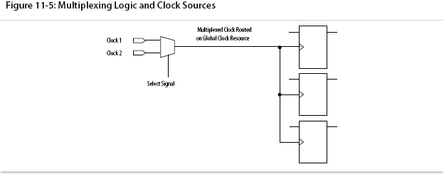
Adding multiplexing logic to the clock signal can create the problems addressed in the previous sections, but requirements for multiplexed clocks vary widely, depending on the application. Clock multiplexing is acceptable when the clock signal uses global clock routing resources and if the following criteria are met:
• The clock multiplexing logic does not change after initial configuration
• The design uses multiplexing logic to select a clock for testing purposes
• Registers are always reset when the clock switches
• A temporarily incorrect response following clock switching has no negative consequences
Use Gated Clocks
Gated clocks turn a clock signal on and off using an enable signal that controls gating circuitry.
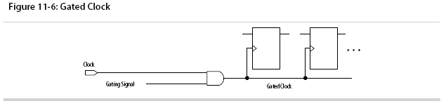
You can use gated clocks to reduce power consumption in some device architectures by effectively shutting down portions of a digital circuit when they are not in use. When a clock is gated, both the clock network and the registers driven by it stop toggling, thereby eliminating their contributions to power consumption. However, gated clocks are not part of a synchronous scheme and therefore can significantly increase the effort required for design implementation and verification. Gated clocks contribute to clock skew and make device migration difficult. These clocks are also sensitive to glitches, which can cause design failure.
Use dedicated hardware to perform clock gating rather than an AND or OR gate.
From a functional point of view, you can shut down a clock domain in a purely synchronous manner using a synchronous clock enable signal.
Use Synchronous Clock Enables
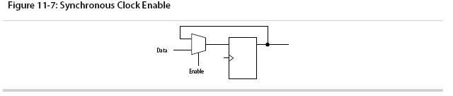
To turn off a clock domain in a synchronous manner, use a synchronous clock enable signal. FPGAs efficiently support clock enable signals because there is a dedicated clock enable signal available on all device registers.
This scheme does not reduce power consumption as much as gating the clock at the source because the clock network keeps toggling, and performs the same function as a gated clock by disabling a set of registers. Insert a multiplexer in front of the data input of every register to either load new data, or copy the output of the register.
Recommended Clock-Gating Methods
Use gated clocks only when your target application requires power reduction and when gated clocks are able to provide the required reduction in your device architecture.
If you must use clocks gated by logic, implement these clocks using the robust clock-gating technique and ensure that the gated clock signal uses dedicated global clock routing.
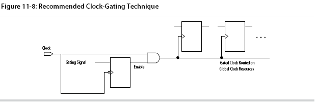
The register that generates the enable signal is triggered on the inactive edge of the clock to be gated. Use the falling edge when gating a clock that is active on the rising edge. Using this technique, only one input of the gate that turns the clock on and off changes at a time. This prevents glitches or spikes on the output.
推荐 的FPGA设计经验(2)-时钟策略优化的更多相关文章
- 推荐 的FPGA设计经验(4) 时钟和寄存器控制架构特性使用
Use Clock and Register-Control Architectural Features FPGAs provide device-wide clocks and register ...
- 推荐 的FPGA设计经验(3) 物理实现和时间闭环优化
Optimizing Physical Implementation and Timing Closure Planning Physical Implementation When planning ...
- 推荐 的FPGA设计经验(1)组合逻辑优化
主要内容摘自Quartus prime Recommended Design Practices For optimal performance, reliability, and faster ti ...
- 【转载】如何在FPGA设计环境中添加加时序约束
转自:http://bbs.ednchina.com/BLOG_ARTICLE_198929.HTM 如何在FPGA设计环境中加时序约束 在给FPGA做逻辑综合和布局布线时,需要在工具中设定时序 ...
- FPGA异步时钟设计中的同步策略
1 引言 基于FPGA的数字系统设计中大都推荐采用同步时序的设计,也就是单时钟系统.但是实际的工程中,纯粹单时钟系统设计的情况很少,特别是设计模块与外围芯片的通信中,跨时钟域的情况经常不可避免. ...
- 影响FPGA设计中时钟因素的探讨。。。转
http://www.fpga.com.cn/advance/skill/speed.htm http://www.fpga.com.cn/advance/skill/design_skill3.ht ...
- FPGA分频与倍频的简单总结(涉及自己设计,调用时钟IP核,调用MMCM原语模块)
原理介绍 1.分频 FPGA设计中时钟分频是重要的基础知识,对于分频通常是利用计数器来实现想要的时钟频率,由此可知分频后的频率周期更大.一般而言实现偶数系数的分频在程序设计上较为容易,而奇数分频则相对 ...
- FPGA设计思想与技巧(转载)
题记:这个笔记不是特权同学自己整理的,特权同学只是对这个笔记做了一下完善,也忘了是从那DOWNLOAD来的,首先对整理者表示感谢.这些知识点确实都很实用,这些设计思想或者也可以说是经验吧,是很值得每一 ...
- 【设计经验】2、ISE中ChipScope使用教程
一.软件与硬件平台 软件平台: 操作系统:Windows 8.1 开发套件:ISE14.7 硬件平台: FPGA型号:XC6SLX45-CSG324 二.ChipScope介绍 ChipScope是X ...
随机推荐
- 解决Ubuntu启动错误——kernel panic not syncing vfs unable to mount root fs on unknown-block 0 0 – error
最近在倒腾Ubuntu,然后想着怎么美化一下界面,于是照着网上的教程整了一下Flatabulous这个软件,然后好像/boot就满了.关机之后再开机就出现了如题所述的错误,无法开机,也无法进入reco ...
- phoneGap的Android下编写phonegap 插件
一. javascript 端的编写 第一个参数 成功的回调函数 第二个参数 失败的回调函数 第三个参数 是插件的类名称,也就是后台java文件的类名 第四个参数 执行的 action 名称 ...
- python SQL注入测试脚本(更新中)
import requests import json import warnings warnings.filterwarnings("ignore") url = 'https ...
- BZOJ 2120 数颜色 【带修改莫队】
任意门:https://www.lydsy.com/JudgeOnline/problem.php?id=2120 2120: 数颜色 Time Limit: 6 Sec Memory Limit: ...
- git忽略文件留存
##ignore this file##/target/ .classpath.project.settings /.settings/ ##filter databfile.sln file##*. ...
- java三大特性(封装、继承、多态)
oop(面向对象程序设计)具有三大特性:封装.继承.多态 一.封装 封装就是讲类的信息隐藏在类的内部,不允许外部程序直接访问,而是通过该类的实现隐藏信息的操作和访问. 实现封装 1.需要修改属性的访问 ...
- ARM Linux 内核 panic 之cache 一致性 ——Cortex-A9多核cache和TLB一致性广播
ARM Linux 内核 panic 之cache 一致性 ——Cortex-A9多核cache和TLB一致性广播 Cortex-A9的多喝CPU可以接收和执行一致性广播操作,当其使能并处于SMP模式 ...
- 一点一点看JDK源码(四)java.util.ArrayList 中篇
一点一点看JDK源码(四)java.util.ArrayList 中篇 liuyuhang原创,未经允许禁止转载 本文举例使用的是JDK8的API 目录:一点一点看JDK源码(〇) 1.综述 在前篇中 ...
- python类的使用(类定义,构造器,类属性,方法)
注:这里只描述使用方法,具体类的概念长篇大论就不要为难我这个懒人了. 总之一句话编程语言只是一个工具,会用就行,好用就行.打破砂锅问到底,我觉得有必要研究一下C,汇编,电子链路等. class clt ...
- Qt5应用程序封包
系统环境:windows10+vs2017+qt5.12 目的:生成.exe可执行文件. 步骤: 1.选择release模式,生成解决方案. 2.打开命令行,cd到生成的可执行文件.exe目录下 3. ...