功率开关管的转换效率:IRFP系列MOSFET@Vishay +SiC碳化硅MOSFET@Infinion+ROHM +GaS氮化镓MOSFET@Microchip+Infinion+Wolfspeed+GanSystem
Vishay Intertechnology
[PDF]High-Voltage Silicon MOSFETs, GaN, and SiC: All have a place
WebPhilip Zuk, Director of Market Development, High-Voltage MOSFET Group, Vishay
GaN vs. SiC: Everything You Need To Know, March 30, 2020 Editorial Staff
IGBT: 97.4% 桥式并联双IGBT(STGW60H65DGB),5KW总热功133W风扇必要.
MOSFET: >97.4% 桥式并联双MOSFET(IRFP460),最好有风扇.
IRFP460, Vds=500V, Id=20A(20°,Vgs=10V, Rgs=0.7Ω, 热功率Phot=I²R=280W),
散热好的桥式双管可承8000W有余。淘宝店价格10元/支上下。
SiC碳化硅MOSFET > 99.00%(超低内阻Rds=0.007Ω, 为常规MOSFET的1/100)
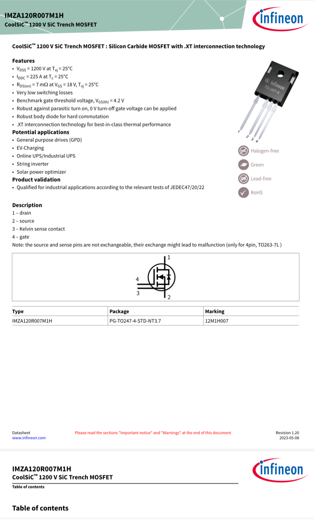
Infinion的CoolSiC硅化碳系列:
IMZA120R007M1H,90美元/支, Vds=1200V, Rds=0.007Ω, 热功率Phot=I²R=280W, Id-max@25°C=225A
即100A的Id时热功率只有70W, 而其正常工作范围:Vds∈[0V,1200V], Id∈[0A,500A]
Advantages
In particular, SiC devices withstand higher voltages, up to 1200V and more,
while GaN devices can withstand lower voltages and power densities;
on the other hand, thanks to the almost zero switch-off times of the GaN devices (high electron mobility with consequent dV/dt greater than 100V/s compared to the 50V/s of the MOSFET Si), these can be used in very high-frequency applications, with unprecedented efficiency and performance. This ideally positive characteristic could prove to be inconvenient: if the parasitic capacitances of the component are not close to zero, current spikes of the order of tens of amperes can be generated, which could cause problems in the electromagnetic compatibility test phase.
SiCs have further advantages on the packages used, due to the possibility of adopting TO-247 and TO-220 which allows the rapid replacement of IGBTs and MOSFETs with the new SiCs, while the GaNs give better results with SMD packages (that are lighter and small but relegated to new projects).
Common design challenges
On the other hand, a common challenge for the two types of devices is related to the design and the construction of gate drivers capable of making the best use of the components-specific characteristics, paying attention to the parasitic components (which must be minimized in order to avoid a weaker performance) and to the levels of applicable voltage (hopefully similar to those used to drive classic silicon components).
Cost differences
In terms of costs, SiC devices are now cheaper and more popular, also because they were made before GaN. However, as it is easy to confirm, costs are only in part related to the production process, and to the market demands, that is why prices will be likely to flatten in the market.
Due to the higher production costs of the GaN substrate, devices that use a GaN “channel” have a Si substrate. In recent months, the Swedish University of Linköping, in collaboration with its spin-off SweGaN, has conducted some research following the idea of using a SiC substrate and a new wafer growth process (called transmorphic heteroepitaxy, which prevents the presence of structural defects), thus obtaining maximum voltages comparable to SiC devices, but capable of working at the frequency of GaN on Si. This research also highlighted how the adoption of this mechanism is able to provide improvements in heat management, a vertical breakdown voltage over 3kV, and a resistance in the ON state less than an order of magnitude compared to today's solutions.
Applications and market share
WBG devices fields of application are still a niche, and R&D still have to better understand how to make the most out of their potential. The largest new technology market is the diode market, but WBG is expected to flood the transistor market over the next 5 years.
Possible applications have started to be hypothesized, and the projections show that electric mobility, telecommunications, and the consumer market are the most plausible.
According to sales forecasts, the most profitable market will be the one involving electric mobility and self-driving vehicles, where the WBG will be used in inverters, onboard charging devices (OBC) and anti-collision systems (LiDAR) and this is obvious, given the thermal characteristics and efficiency of the new devices that matches with the request to optimize the performance of the accumulators.
As for telecommunications, the role of 5G will be the driving force for the WBG, whose millions of stations to be installed will need higher energy efficiency, and will also be smaller and lighter, with a significant gain in performance and cuts on costs.
The consumer market will also involve the massive use of new devices. Wireless power and recharging devices will be mainly affected, thanks to the ever-increasing spread of mobile devices and therefore to the needs of fast-charging.
SiC and GaN devices
Infineon has developed a wide range of SiC and GaN MOSFET devices with their drivers, the CoolSiC and CoolGaN series. Noteworthy is the FF6MR12W2M1_B11 half-bridge module, which is capable of delivering up to 200A at 1200V, with an RDS(on) resistance of only 6mΩ. The module is equipped with two SiC MOSFETs and a NTC temperature sensor, and is suitable for UPS and motor control applications, with an eye to efficiency and thermal dissipation (figure 1).
There is a similar solution in the Microsemi catalog (now Microchip Technology), with the Phase Leg SiC MOSFET module, which makes use of the SP6LI devices family, and allows voltages up to 1700V and currents greater than 200A; the AlN substrate ensures better thermal management, and two SiC Schottky diodes allow for an increase in switching frequencies.
Wolfspeed is keeping up with the market with its CAB450M12XM3, half-bridge device capable of managing voltages up to 1200V and currents of 450A, suitable for working up to 175°C in continuous mode thanks to the use of their third generation MOSFETs with SiN substrate.
When taking a look at the GaN world, it is immediately clear that a variety of devices available is limited. GanSystem offers the GS-065-150-1-D in its catalog, a transistor that makes use of the patented Island Technology, capable of managing up to 650V and 150A at a switching frequency greater than 10MHz.
Finally, with its TP90H050WS FET, which will see the light in mid-2020, Transphorm is working on a GaN device using the TO-247 package whose working voltage can reach 900V, with rising and falling times of about 10nS (Figure 2).

Figure 1: FF6MR12W2M1_B11 half-bridge module
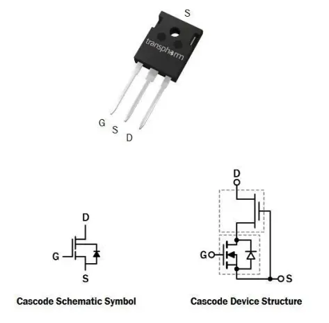
Figure 2: TP90H050WS FET
By Davide Di Gesuald
Related articles:
- GaN vs. SiC Transistors
- Gallium Oxide, a New Generation of Semiconductor Material for Power Devices
- What makes SiC and GaN suitable for high-power designs
@ROHM的能源转换效率甚至高达99%,可无风扇散热!
ROHM官方的Application Note(Issued 2021)
SiC MOSFET: 开关频率可以倍增,平滑滤波电感器可小型化、尺寸和重量减半。
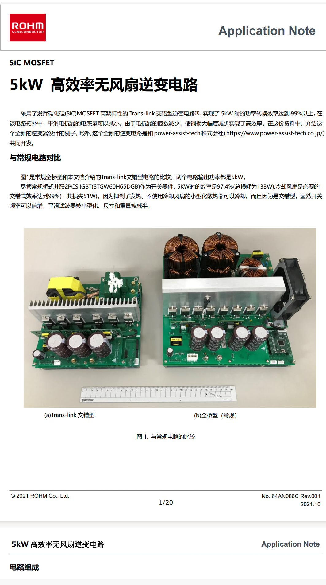
5kW 高效率无风扇逆变电路
采用了发挥碳化硅(SiC)MOSFET 高频特性的 Trans-link 交错型逆变电路(1)、实现了 5kW 时的功率转换效率达到 99%以上。在该电路的拓扑,平滑电感器的电感量可以减小。由于电感器的匝数减少、使功损大幅度减少实现了高效率。
这份资料介绍这个全新的逆变器设计例子。此外,这个全新的逆变电路是和 power-assist-tech 株式会社(https://www.power-assist-tech.co.jp/)共同开发。
与常规电路对比图1是常规全桥型和本文档介绍的Trans-link交叉型电路的比较,两个电路输出功率都是5kW。尽管常规桥式并联2PCS IGBT(STGW60H65DGB)作为开关器件,5KW时的效率是97.4%(总损耗为133W),冷却风扇是必要的。
交叉式效率达到99%(一共损失51W),因为抑制了发热、不使用冷却风扇的小型化散热器可以冷却。而且因为是交叉型,开关频率可以倍增,平滑滤波器被小型化、尺寸和重量被减半。
功率开关管的转换效率:IRFP系列MOSFET@Vishay +SiC碳化硅MOSFET@Infinion+ROHM +GaS氮化镓MOSFET@Microchip+Infinion+Wolfspeed+GanSystem的更多相关文章
- 【雕爷学编程】Arduino动手做(56)---8路LED跑马灯模块
37款传感器与模块的提法,在网络上广泛流传,其实Arduino能够兼容的传感器模块肯定是不止37种的.鉴于本人手头积累了一些传感器和模块,依照实践出真知(一定要动手做)的理念,以学习和交流为目的,这里 ...
- STM32 基于 CubeMX配置GPIO点亮LED灯(超级详细+图文并茂)
我是一个只会点灯的菜鸟: 相关文章 [STM32系列汇总]小白博主的STM32实战快速进阶之路(持续更新) 文章目录 相关文章 1 前言 2 理论分析 2.1 LED 原理 2.2 板载资料 2.3 ...
- MOSFET, MOS管, 开关管笔记
MOSFET, MOS管, 开关管 MOSFET, Metal-Oxide-Semiconductor Field-Effect Transistor, 金属氧化物半导体场效晶体管 常见封装 电路符号 ...
- Buck工作原理分析,连续模式,断续模式
Part01:Buck电路工作原理: 图1-1 Buck电路拓扑结构 Buck电路的拓扑结构如图1-1所示: (1) input接输入电源,既直流电动势: (2) IGBT1为开关管,可以选择以全控型 ...
- 基于TDA4863-2的单级PFC反激LED电源设计与仿真
LED是一个非线性器件,正向电压的微小变化会引起电流的巨大变化:LED是一个半导体二极管,其伏安特性随温度变化而变化(-2mV/℃),假如温度升高,在恒压驱动下LED的电流会增加.长期超过额定电流工作 ...
- [Fundamental of Power Electronics]-PART I-4.开关实现-4.2 功率半导体器件概述
4.2 功率半导体器件概述 功率半导体设计中最根本的挑战是获得高击穿电压,同时保持低正向压降和导通电阻.一个密切相关的问题是高压低导通电阻器件的开关时间更长.击穿电压,导通电阻和开关时间之间的折衷是各 ...
- Transistor 晶体管 场效应 双极型 达林顿 CMOS PMOS BJT FET
Transistor Tutorial Summary Transistor Tutorial Summary Bipolar Junction Transistor Tutorial We can ...
- IIC双向电平转换电路设计
现代的集成电路工艺加工的间隙可达0.5μm 而且很少限制数字I/O 信号的最大电源电压和逻辑电平. 为了将这些低电压电路与已有的5V或其他I/O电压器件连接起来,接口需要一个电平转换器.对于双向的总线 ...
- DG449 High Voltage Single SPDT Analog Switch in SOT23-8
DESCRIPTION The DG449 is a dual supply single-pole/double-throw (SPDT) switches. On resistance is 38 ...
- PFC电源设计与电感设计计算学习笔记
PFC电源设计与电感设计计算 更新于2018-11-30 课程概览 常见PFC电路和特点1 常见PFC电路和特点1 CRM PFC电路设计计算 CCM PFC电路设计计算 CCM Interleave ...
随机推荐
- Rust实战系列-生命周期、所有权和借用
本文是<Rust in action>学习总结系列的第四部分,更多内容请看已发布文章: 一.Rust实战系列-Rust介绍 二.Rust实战系列-基本语法 三.Rust实战系列-复合数据类 ...
- Python3_数据类型和变量
Python3_数据类型和变量 一.数据类型 Python有五个标准的数据类型: Numbers(数字) String(字符串) List(列表) Tuple(元组) Dictionary(字典) 在 ...
- NOIP集训 P11071 「QMSOI R1」 Distorted Fate 题解
对本题的评价:有思维含量的线段树好题.曲子好听,曲绘好看,曲师人品好,谱子写得好,鸠好看 题解: P11071 「QMSOI R1」 Distorted Fate 给定一个长度为 \(n\) 的数组 ...
- 『Plotly实战指南』--在金融数据可视化中的应用(下)
在金融市场的复杂博弈中,可视化技术如同精密的导航仪. 传统静态图表正在被交互式可视化取代--据Gartner研究,采用动态可视化的投资机构决策效率提升达47%. 本文的目标是探讨如何利用 Plotly ...
- 漏洞预警 | CraftCMS模板注入漏洞
0x00 漏洞编号 CVE-2024-56145 0x01 危险等级 高危 0x02 漏洞概述 CraftCMS是一个灵活的.易于使用的内容管理系统. 0x03 漏洞详情 CVE-2024-56145 ...
- 轮播图导航组件 | 纯血鸿蒙组件库AUI
摘要: 轮播图导航(A_SwiperNav):实现沉浸式体验的App全屏轮播引导页效果.可设置图片数据(含文本.图片地址.路由.标题.子标题),可设置按钮颜色. 一.在页面当中调用轮播图导航组件 打开 ...
- P2779 [AHOI2016初中组] 黑白序列题解
题意: 小可可准备了一个未完成的黑白序列,用 B 和 W 表示黑色和白色,用 ? 表示尚未确定. 他希望知道一共有多少种不同的方法,在决定了每一个 ? 位置的颜色后可以得到一个小雪喜欢的黑白序列. 其 ...
- LR_GD_MSE (公式补充)
上篇是先撸了一把梯度下降的代码, 用来优先 LR 中的 MSE. 核心代码是在求解梯度这一步. # y = wx + b def step_gradient(b_current, w_current, ...
- C++ decltype类型推导
1.decltype介绍 decltype(declare type,声明类型)为C++11 新增的关键字,和auto功能一样,用于在编译期间进行自动类型推导. auto和decltype关键字都可以 ...
- C++ ADL 与 模板
什么是ADL ADL(Argument Dependent Lookup),参数依赖查找,明确的意思是依赖参数的函数查找,即对于函数调用,不仅会依照常规的名称查找规则,还会在函数参数所在的命名空间内查 ...