单片机成长之路(51基础篇) - 023 N76e003 系统时钟切换到外部时钟
N76e003切换到外部时钟的资料很少(因为N76e003的片子是不支持无源晶振的,有源晶振的成本又很高,所以网上很少有对N76e003的介绍)。有图有真相:
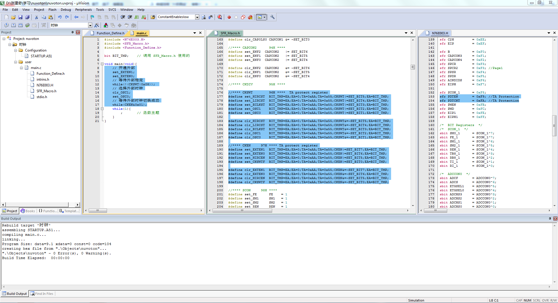
代码如下:
main.c
 #include <N76E003.H>

 #include <SFR_Macro.h>

 #include <Function_Define.h>

 bit BIT_TMP;    // 调用 SFR_Macro.h 使用的

 void main(void){

     // 开通外部

     set_EXTEN1;

     set_EXTEN0;

     // 等待外部稳定

     while(!(CKSWT|0x08));

     // 选择外部时钟

     clr_OSC1;

     set_OSC0;

     // 等待外部时钟切换成功

     while(CKEN&0x01);

     while(){

         ;        // 函数主题

     }

 }
 /*--------------------------------------------------------------------------

 N76E003.H

 Header file for Nuvoton N76E003

 --------------------------------------------------------------------------*/

 #ifndef __N76E885_H__

 #define __N76E885_H__

 sfr P0          = 0x80;

 sfr SP          = 0x81;

 sfr DPL         = 0x82;

 sfr DPH         = 0x83;

 sfr RWK         = 0x86;

 sfr PCON        = 0x87;

 sfr TCON        = 0x88;

 sfr TMOD        = 0x89;

 sfr TL0         = 0x8A;

 sfr TL1         = 0x8B;

 sfr TH0         = 0x8C;

 sfr TH1         = 0x8D;

 sfr CKCON       = 0x8E;

 sfr WKCON       = 0x8F;

 sfr P1          = 0x90;

 sfr SFRS        = 0x91; //TA Protection

 sfr CAPCON0     = 0x92;

 sfr CAPCON1     = 0x93;

 sfr CAPCON2     = 0x94;

 sfr CKDIV       = 0x95;

 sfr CKSWT       = 0x96; //TA Protection

 sfr CKEN        = 0x97; //TA Protection

 sfr SCON        = 0x98;

 sfr SBUF        = 0x99;

 sfr SBUF_1      = 0x9A;

 sfr EIE         = 0x9B;

 sfr EIE1        = 0x9C;

 sfr CHPCON      = 0x9F; //TA Protection

 sfr P2          = 0xA0;

 sfr AUXR1       = 0xA2;

 sfr BODCON0     = 0xA3; //TA Protection

 sfr IAPTRG      = 0xA4; //TA Protection

 sfr IAPUEN      = 0xA5;    //TA Protection

 sfr IAPAL       = 0xA6;

 sfr IAPAH       = 0xA7;

 sfr IE          = 0xA8;

 sfr SADDR       = 0xA9;

 sfr WDCON       = 0xAA; //TA Protection

 sfr BODCON1     = 0xAB; //TA Protection

 sfr P3M1        = 0xAC;

 sfr P3S         = 0xAC; //Page1

 sfr P3M2        = 0xAD;

 sfr P3SR        = 0xAD; //Page1

 sfr IAPFD       = 0xAE;

 sfr IAPCN       = 0xAF;

 sfr P3          = 0xB0;

 sfr P0M1        = 0xB1;

 sfr P0S         = 0xB1; //Page1

 sfr P0M2        = 0xB2;

 sfr P0SR        = 0xB2; //Page1

 sfr P1M1        = 0xB3;

 sfr P1S         = 0xB3; //Page1

 sfr P1M2        = 0xB4;

 sfr P1SR        = 0xB4; //Page1

 sfr P2S         = 0xB5;

 sfr IPH         = 0xB7;

 sfr PWMINTC        = 0xB7;    //Page1

 sfr IP          = 0xB8;

 sfr SADEN       = 0xB9;

 sfr SADEN_1     = 0xBA;

 sfr SADDR_1     = 0xBB;

 sfr I2DAT       = 0xBC;

 sfr I2STAT      = 0xBD;

 sfr I2CLK       = 0xBE;

 sfr I2TOC       = 0xBF;

 sfr I2CON       = 0xC0;

 sfr I2ADDR      = 0xC1;

 sfr ADCRL       = 0xC2;

 sfr ADCRH       = 0xC3;

 sfr T3CON       = 0xC4;

 sfr PWM4H       = 0xC4; //Page1

 sfr RL3         = 0xC5;

 sfr PWM5H       = 0xC5;    //Page1

 sfr RH3         = 0xC6;

 sfr PIOCON1     = 0xC6; //Page1

 sfr TA          = 0xC7;

 sfr T2CON       = 0xC8;

 sfr T2MOD       = 0xC9;

 sfr RCMP2L      = 0xCA;

 sfr RCMP2H      = 0xCB;

 sfr TL2         = 0xCC;

 sfr PWM4L       = 0xCC; //Page1

 sfr TH2         = 0xCD;

 sfr PWM5L       = 0xCD; //Page1

 sfr ADCMPL      = 0xCE;

 sfr ADCMPH      = 0xCF;

 sfr PSW         = 0xD0;

 sfr PWMPH       = 0xD1;

 sfr PWM0H        = 0xD2;

 sfr PWM1H        = 0xD3;

 sfr PWM2H        = 0xD4;

 sfr PWM3H        = 0xD5;

 sfr PNP            = 0xD6;

 sfr FBD            = 0xD7;

 sfr PWMCON0        = 0xD8;

 sfr PWMPL       = 0xD9;

 sfr PWM0L        = 0xDA;

 sfr PWM1L        = 0xDB;

 sfr PWM2L        = 0xDC;

 sfr PWM3L        = 0xDD;

 sfr PIOCON0        = 0xDE;

 sfr PWMCON1     = 0xDF;

 sfr ACC         = 0xE0;

 sfr ADCCON1     = 0xE1;

 sfr ADCCON2     = 0xE2;

 sfr ADCDLY      = 0xE3;

 sfr C0L         = 0xE4;

 sfr C0H         = 0xE5;

 sfr C1L         = 0xE6;

 sfr C1H         = 0xE7;

 sfr ADCCON0     = 0xE8;

 sfr PICON       = 0xE9;

 sfr PINEN       = 0xEA;

 sfr PIPEN       = 0xEB;

 sfr PIF         = 0xEC;

 sfr C2L         = 0xED;

 sfr C2H         = 0xEE;

 sfr EIP         = 0xEF;

 sfr B           = 0xF0;

 sfr CAPCON3        = 0xF1;

 sfr CAPCON4        = 0xF2;

 sfr SPCR        = 0xF3;

 sfr SPCR2        = 0xF3; //Page1

 sfr SPSR        = 0xF4;

 sfr SPDR        = 0xF5;

 sfr AINDIDS        = 0xF6;

 sfr EIPH        = 0xF7;

 sfr SCON_1      = 0xF8;

 sfr PDTEN       = 0xF9; //TA Protection

 sfr PDTCNT      = 0xFA; //TA Protection

 sfr PMEN        = 0xFB;

 sfr PMD         = 0xFC;

 sfr EIP1        = 0xFE;

 sfr EIPH1       = 0xFF;

 /*  BIT Registers  */

 /*  SCON_1  */

 sbit SM0_1      = SCON_1^;

 sbit FE_1       = SCON_1^;

 sbit SM1_1      = SCON_1^;

 sbit SM2_1      = SCON_1^;

 sbit REN_1      = SCON_1^;

 sbit TB8_1      = SCON_1^;

 sbit RB8_1      = SCON_1^;

 sbit TI_1       = SCON_1^;

 sbit RI_1       = SCON_1^;

 /*  ADCCON0  */

 sbit ADCF       = ADCCON0^;

 sbit ADCS       = ADCCON0^;

 sbit ETGSEL1    = ADCCON0^;

 sbit ETGSEL0    = ADCCON0^;

 sbit ADCHS3     = ADCCON0^;

 sbit ADCHS2     = ADCCON0^;

 sbit ADCHS1     = ADCCON0^;

 sbit ADCHS0     = ADCCON0^;

 /*  PWMCON0  */

 sbit PWMRUN     = PWMCON0^;

 sbit LOAD       = PWMCON0^;

 sbit PWMF       = PWMCON0^;

 sbit CLRPWM     = PWMCON0^;

 /*  PSW */

 sbit CY         = PSW^;

 sbit AC         = PSW^;

 sbit F0         = PSW^;

 sbit RS1        = PSW^;

 sbit RS0        = PSW^;

 sbit OV         = PSW^;

 sbit P          = PSW^;

 /*  T2CON  */

 sbit TF2        = T2CON^;

 sbit TR2        = T2CON^;

 sbit CM_RL2     = T2CON^;

 /*  I2CON  */

 sbit I2CEN      = I2CON^;

 sbit STA        = I2CON^;

 sbit STO        = I2CON^;

 sbit SI         = I2CON^;

 sbit AA         = I2CON^;

 sbit I2CPX    = I2CON^;

 /*  IP  */

 sbit PADC       = IP^;

 sbit PBOD       = IP^;

 sbit PS         = IP^;

 sbit PT1        = IP^;

 sbit PX1        = IP^;

 sbit PT0        = IP^;

 sbit PX0        = IP^;

 /*  P3  */

 sbit P30        = P3^;

 /*  IE  */

 sbit EA         = IE^;

 sbit EADC       = IE^;

 sbit EBOD       = IE^;

 sbit ES         = IE^;

 sbit ET1        = IE^;

 sbit EX1        = IE^;

 sbit ET0        = IE^;

 sbit EX0        = IE^;

 /*  P2  */

 sbit P20        = P2^;

 /*  SCON  */

 sbit SM0        = SCON^;

 sbit FE         = SCON^;

 sbit SM1        = SCON^;

 sbit SM2        = SCON^;

 sbit REN        = SCON^;

 sbit TB8        = SCON^;

 sbit RB8        = SCON^;

 sbit TI         = SCON^;

 sbit RI         = SCON^;

 /*  P1  */

 sbit P17    = P1^;

 sbit AIN0    = P1^;

 sbit P10        = P1^;

 sbit PWM0       = P1^;

 sbit P11        = P1^;

 sbit PWM1       = P1^;

 sbit P12        = P1^;

 /*  TCON  */

 sbit TF1        = TCON^;

 sbit TR1        = TCON^;

 sbit TF0        = TCON^;

 sbit TR0        = TCON^;

 sbit IE1        = TCON^;

 sbit IT1        = TCON^;

 sbit IE0        = TCON^;

 sbit IT0        = TCON^;

 /*  P0  */

 sbit P00        = P0^;

 sbit INT0       = P0^;

 sbit VREF       = P0^;

 sbit P01        = P0^;

 sbit INT1       = P0^;

 sbit AIN1       = P0^;

 sbit P02        = P0^;

 sbit PWM2       = P0^;

 sbit AIN2       = P0^;

 sbit P03        = P0^;

 sbit PWM3       = P0^;

 sbit TXD        = P0^;

 sbit AIN3       = P0^;

 sbit P04        = P0^;

 sbit SS         = P0^;

 sbit AIN4       = P0^;

 sbit P05        = P0^;

 sbit PWM4       = P0^;

 sbit SPICK      = P0^;

 sbit AIN5       = P0^;

 sbit P06        = P0^;

 sbit SCL        = P0^;

 sbit AIN6       = P0^;

 sbit PWM5       = P0^;

 sbit P07        = P0^;

 sbit AIN7       = P0^;

 sbit PWM6       = P0^;

 #endif
/**** P0 80H *****/
#define set_P00 P00 = 1
#define set_P01 P01 = 1
#define set_P02 P02 = 1
#define set_P03 P03 = 1
#define set_P04 P04 = 1
#define set_P05 P05 = 1
#define set_P06 P06 = 1
#define set_P07 P07 = 1 #define clr_P00 P00 = 0
#define clr_P01 P01 = 0
#define clr_P02 P02 = 0
#define clr_P03 P03 = 0
#define clr_P04 P04 = 0
#define clr_P05 P05 = 0
#define clr_P06 P06 = 0
#define clr_P07 P07 = 0 //**** SP 81H ****
//**** DPH 82H ****
//**** DPL 83H ****
//**** RWK 86H **** //**** PCON 87H *****
#define set_SMOD PCON |= SET_BIT7
#define set_SMOD0 PCON |= SET_BIT6
#define set_POF PCON |= SET_BIT4
#define set_GF1 PCON |= SET_BIT3
#define set_GF0 PCON |= SET_BIT2
#define set_PD PCON |= SET_BIT1
#define set_IDL PCON |= SET_BIT0 #define clr_SMOD PCON &= ~SET_BIT7
#define clr_SMOD0 PCON &= ~SET_BIT6
#define clr_POF PCON &= ~SET_BIT4
#define clr_GF1 PCON &= ~SET_BIT3
#define clr_GF0 PCON &= ~SET_BIT2
#define clr_PD PCON &= ~SET_BIT1
#define clr_IDL PCON &= ~SET_BIT0 /**** TCON 88H ****/
#define set_TF1 TF1 = 1
#define set_TR1 TR1 = 1
#define set_TF0 TF0 = 1
#define set_TR0 TR0 = 1 //启动定时器0(定时器0启动控制,0定时器0终止,清除该位将终止定时器0并且当前计数值将保存到TH0和TL0中,1使能定时器0)
#define set_IE1 IE1 = 1
#define set_IT1 IT1 = 1
#define set_IE0 IE0 = 1
#define set_IT0 IT0 = 1 #define clr_TF1 TF1 = 0
#define clr_TR1 TR1 = 0
#define clr_TF0 TF0 = 0
#define clr_TR0 TR0 = 0
#define clr_IE1 IE1 = 0
#define clr_IT1 IT1 = 0
#define clr_IE0 IE0 = 0
#define clr_IT0 IT0 = 0 //**** TMOD 89H ****
#define set_GATE_T1 TMOD |= SET_BIT7
#define set_CT_T1 TMOD |= SET_BIT6
#define set_M1_T1 TMOD |= SET_BIT5
#define set_M0_T1 TMOD |= SET_BIT4
#define set_GATE_T0 TMOD |= SET_BIT3
#define set_CT_T0 TMOD |= SET_BIT2
#define set_M1_T0 TMOD |= SET_BIT1
#define set_M0_T0 TMOD |= SET_BIT0 #define clr_GATE_T1 TMOD &= ~SET_BIT7
#define clr_CT_T1 TMOD &= ~SET_BIT6
#define clr_M1_T1 TMOD &= ~SET_BIT5
#define clr_M0_T1 TMOD &= ~SET_BIT4
#define clr_GATE_T0 TMOD &= ~SET_BIT3
#define clr_CT_T0 TMOD &= ~SET_BIT2
#define clr_M1_T0 TMOD &= ~SET_BIT1
#define clr_M0_T0 TMOD &= ~SET_BIT0 //**** TH1 8AH ****
//**** TH0 8BH ****
//**** TL1 8CH ****
//**** TL0 8DH **** //CKCON - 8EH 时钟控制寄存器
#define set_PWMCKS CKCON |= SET_BIT6 //设置pwm时钟源为定时器1的溢出(0为系统时钟,1为定时器1的溢出)
#define set_T1M CKCON |= SET_BIT4 //设置定时器1的时钟为系统时钟(0为1/12系统时钟,与8051兼容,1为选择时钟源为系统时钟)
#define set_T0M CKCON |= SET_BIT3 //设置定时器0的时钟为系统时钟(0为1/12系统时钟,与8051兼容,1为选择时钟源为系统时钟)
#define set_CLOEN CKCON |= SET_BIT1 //设置系统时钟输出使能,从PLO(P1.1)输出(0禁用系统时钟输出,1使系统时钟创覲LO(P1.1)输出)
//清除时钟
#define clr_PWMCKS CKCON &= ~SET_BIT6 //设置pwm时钟源为系统时钟(0为系统时钟,1为定时器1的溢出)
#define clr_T1M CKCON &= ~SET_BIT4 //设置定时器1的时钟为1/12系统时钟(0为1/12系统时钟,与8051兼容,1为选择时钟源为系统时钟)
#define clr_T0M CKCON &= ~SET_BIT3 //设置定时器0的时钟为1/12系统时钟(0为1/12系统时钟,与8051兼容,1为选择时钟源为系统时钟)
#define clr_CLOEN CKCON &= ~SET_BIT1 //设置系统时钟输出使能,禁用系统时钟输出(0禁用系统时钟输出,1使系统时钟创覲LO(P1.1)输出) //**** WKCON 8FH ****
#define set_WKTCK WKCON |= SET_BIT5
#define set_WKTF WKCON |= SET_BIT4
#define set_WKTR WKCON |= SET_BIT3
#define set_WKPS2 WKCON |= SET_BIT2
#define set_WKPS1 WKCON |= SET_BIT1
#define set_WKPS0 WKCON |= SET_BIT0 #define clr_WKTCK WKCON &= ~SET_BIT5
#define clr_WKTF WKCON &= ~SET_BIT4
#define clr_WKTR WKCON &= ~SET_BIT3
#define clr_WKPS2 WKCON &= ~SET_BIT2
#define clr_WKPS1 WKCON &= ~SET_BIT1
#define clr_WKPS0 WKCON &= ~SET_BIT0 /**** P1 90H *****/
#define set_P10 P10 = 1
#define set_P11 P11 = 1
#define set_P12 P12 = 1
#define set_P13 P13 = 1
#define set_P14 P14 = 1
#define set_P15 P15 = 1
#define set_P16 P16 = 1
#define set_P17 P17 = 1 #define clr_P10 P10 = 0
#define clr_P11 P11 = 0
#define clr_P12 P12 = 0
#define clr_P13 P13 = 0
#define clr_P14 P14 = 0
#define clr_P15 P15 = 0
#define clr_P16 P16 = 0
#define clr_P17 P17 = 0 //****SFRS 91H ****
#define set_SFRPAGE BIT_TMP=EA;EA=0;TA=0xAA;TA=0x55;SFRS|=SET_BIT0;EA=BIT_TMP
#define clr_SFRPAGE BIT_TMP=EA;EA=0;TA=0xAA;TA=0x55;SFRS&=~SET_BIT0;EA=BIT_TMP //****CAPCON0 92H ****
#define set_CAPEN2 CAPCON0 |= SET_BIT6
#define set_CAPEN1 CAPCON0 |= SET_BIT5
#define set_CAPEN0 CAPCON0 |= SET_BIT4
#define set_CAPF2 CAPCON0 |= SET_BIT2
#define set_CAPF1 CAPCON0 |= SET_BIT1
#define set_CAPF0 CAPCON0 |= SET_BIT0 #define clr_CAPEN2 CAPCON0 &= ~SET_BIT6
#define clr_CAPEN1 CAPCON0 &= ~SET_BIT5
#define clr_CAPEN0 CAPCON0 &= ~SET_BIT4
#define clr_CAPF2 CAPCON0 &= ~SET_BIT2
#define clr_CAPF1 CAPCON0 &= ~SET_BIT1
#define clr_CAPF0 CAPCON0 &= ~SET_BIT0 //**** CAPCON1 93H ****
#define set_CAP2LS1 CAPCON1 |= SET_BIT5
#define set_CAP2LS0 CAPCON1 |= SET_BIT4
#define set_CAP1LS1 CAPCON1 |= SET_BIT3
#define set_CAP1LS0 CAPCON1 |= SET_BIT2
#define set_CAP0LS1 CAPCON1 |= SET_BIT1
#define set_CAP0LS0 CAPCON1 |= SET_BIT0 #define clr_CAP2LS1 CAPCON1 &= ~SET_BIT5
#define clr_CAP2LS0 CAPCON1 &= ~SET_BIT4
#define clr_CAP1LS1 CAPCON1 &= ~SET_BIT3
#define clr_CAP1LS0 CAPCON1 &= ~SET_BIT2
#define clr_CAP0LS1 CAPCON1 &= ~SET_BIT1
#define clr_CAP0LS0 CAPCON1 &= ~SET_BIT0 //**** CAPCON2 94H ****
#define set_ENF2 CAPCON2 |= SET_BIT6
#define set_ENF1 CAPCON2 |= SET_BIT5
#define set_ENF0 CAPCON2 |= SET_BIT4 #define clr_ENF2 CAPCON2 &= ~SET_BIT6
#define clr_ENF1 CAPCON2 &= ~SET_BIT5
#define clr_ENF0 CAPCON2 &= ~SET_BIT4 //**** CKDIV 95H **** //**** CKSWT 96H **** TA protect register
#define set_HIRCST BIT_TMP=EA;EA=0;TA=0xAA;TA=0x55;CKSWT|=SET_BIT5;EA=BIT_TMP;
#define set_LIRCST BIT_TMP=EA;EA=0;TA=0xAA;TA=0x55;CKSWT|=SET_BIT4;EA=BIT_TMP;
#define set_ECLKST BIT_TMP=EA;EA=0;TA=0xAA;TA=0x55;CKSWT|=SET_BIT3;EA=BIT_TMP;
#define set_OSC1 BIT_TMP=EA;EA=0;TA=0xAA;TA=0x55;CKSWT|=SET_BIT2;EA=BIT_TMP;
#define set_OSC0 BIT_TMP=EA;EA=0;TA=0xAA;TA=0x55;CKSWT|=SET_BIT1;EA=BIT_TMP; #define clr_HIRCST BIT_TMP=EA;EA=0;TA=0xAA;TA=0x55;CKSWT&=~SET_BIT5;EA=BIT_TMP;
#define clr_LIRCST BIT_TMP=EA;EA=0;TA=0xAA;TA=0x55;CKSWT&=~SET_BIT4;EA=BIT_TMP;
#define clr_ECLKST BIT_TMP=EA;EA=0;TA=0xAA;TA=0x55;CKSWT&=~SET_BIT3;EA=BIT_TMP;
#define clr_OSC1 BIT_TMP=EA;EA=0;TA=0xAA;TA=0x55;CKSWT&=~SET_BIT2;EA=BIT_TMP;
#define clr_OSC0 BIT_TMP=EA;EA=0;TA=0xAA;TA=0x55;CKSWT&=~SET_BIT1;EA=BIT_TMP; //**** CKEN 97H **** TA protect register
#define set_EXTEN1 BIT_TMP=EA;EA=0;TA=0xAA;TA=0x55;CKEN|=SET_BIT7;EA=BIT_TMP;
#define set_EXTEN0 BIT_TMP=EA;EA=0;TA=0xAA;TA=0x55;CKEN|=SET_BIT6;EA=BIT_TMP;
#define set_HIRCEN BIT_TMP=EA;EA=0;TA=0xAA;TA=0x55;CKEN|=SET_BIT5;EA=BIT_TMP;
#define set_CKSWTF BIT_TMP=EA;EA=0;TA=0xAA;TA=0x55;CKEN|=SET_BIT0;EA=BIT_TMP; #define clr_EXTEN1 BIT_TMP=EA;EA=0;TA=0xAA;TA=0x55;CKEN&=~SET_BIT7;EA=BIT_TMP;
#define clr_EXTEN0 BIT_TMP=EA;EA=0;TA=0xAA;TA=0x55;CKEN&=~SET_BIT6;EA=BIT_TMP;
#define clr_HIRCEN BIT_TMP=EA;EA=0;TA=0xAA;TA=0x55;CKEN&=~SET_BIT5;EA=BIT_TMP;
#define clr_CKSWTF BIT_TMP=EA;EA=0;TA=0xAA;TA=0x55;CKEN&=~SET_BIT0;EA=BIT_TMP; //**** SCON 98H ****
#define set_FE FE = 1
#define set_SM1 SM1 = 1
#define set_SM2 SM2 = 1
#define set_REN REN = 1
#define set_TB8 TB8 = 1
#define set_RB8 RB8 = 1
#define set_TI TI = 1
#define set_RI RI = 1 #define clr_FE FE = 0
#define clr_SM1 SM1 = 0
#define clr_SM2 SM2 = 0
#define clr_REN REN = 0
#define clr_TB8 TB8 = 0
#define clr_RB8 RB8 = 0
#define clr_TI TI = 0
#define clr_RI RI = 0 //**** SBUF 99H ****
//**** SBUF_1 9AH **** //**** EIE 9BH ****
#define set_ET2 EIE |= SET_BIT7
#define set_ESPI EIE |= SET_BIT6
#define set_EFB EIE |= SET_BIT5
#define set_EWDT EIE |= SET_BIT4
#define set_EPWM EIE |= SET_BIT3
#define set_ECAP EIE |= SET_BIT2
#define set_EPI EIE |= SET_BIT1
#define set_EI2C EIE |= SET_BIT0 #define clr_ET2 EIE &= ~SET_BIT7
#define clr_ESPI EIE &= ~SET_BIT6
#define clr_EFB EIE &= ~SET_BIT5
#define clr_EWDT EIE &= ~SET_BIT4
#define clr_EPWM EIE &= ~SET_BIT3
#define clr_ECAP EIE &= ~SET_BIT2
#define clr_EPI EIE &= ~SET_BIT1
#define clr_EI2C EIE &= ~SET_BIT0 //**** EIE1 9CH ****
#define set_EWKT EIE1 |= SET_BIT2
#define set_ET3 EIE1 |= SET_BIT1
#define set_ES_1 EIE1 |= SET_BIT0 #define clr_EWKT EIE1 &= ~SET_BIT2
#define clr_ET3 EIE1 &= ~SET_BIT1
#define clr_ES_1 EIE1 &= ~SET_BIT0 //**** CHPCON 9DH **** TA protect register
#define set_SWRST BIT_TMP=EA;EA=0;TA=0xAA;TA=0x55;CHPCON|=SET_BIT7 ;EA=BIT_TMP
#define set_IAPFF BIT_TMP=EA;EA=0;TA=0xAA;TA=0x55;CHPCON|=SET_BIT6 ;EA=BIT_TMP
#define set_BS BIT_TMP=EA;EA=0;TA=0xAA;TA=0x55;CHPCON|=SET_BIT1 ;EA=BIT_TMP
#define set_IAPEN BIT_TMP=EA;EA=0;TA=0xAA;TA=0x55;CHPCON|=SET_BIT0 ;EA=BIT_TMP #define clr_SWRST BIT_TMP=EA;EA=0;TA=0xAA;TA=0x55;CHPCON&=~SET_BIT7;EA=BIT_TMP
#define clr_IAPFF BIT_TMP=EA;EA=0;TA=0xAA;TA=0x55;CHPCON&=~SET_BIT6;EA=BIT_TMP
#define clr_BS BIT_TMP=EA;EA=0;TA=0xAA;TA=0x55;CHPCON&=~SET_BIT1;EA=BIT_TMP
#define clr_IAPEN BIT_TMP=EA;EA=0;TA=0xAA;TA=0x55;CHPCON&=~SET_BIT0;EA=BIT_TMP //**** P2 A0H **** //**** AUXR1 A2H ****
#define set_SWRF AUXR1 |= SET_BIT7
#define set_RSTPINF AUXR1 |= SET_BIT6
#define set_HARDF AUXR1 |= SET_BIT5
#define set_GF2 AUXR1 |= SET_BIT3
#define set_UART0PX AUXR1 |= SET_BIT2
#define set_DPS AUXR1 |= SET_BIT0 #define clr_SWRF AUXR1 &= ~SET_BIT7
#define clr_RSTPINF AUXR1 &= ~SET_BIT6
#define clr_HARDF AUXR1 &= ~SET_BIT5
#define clr_GF2 AUXR1 &= ~SET_BIT3
#define clr_UART0PX AUXR1 &= ~SET_BIT2
#define clr_DPS AUXR1 &= ~SET_BIT0 //**** BODCON0 A3H **** TA protect register
#define set_BODEN BIT_TMP=EA;EA=0;TA=0xAA;TA=0x55;BODCON0|=SET_BIT7;EA=BIT_TMP
#define set_BOV2 BIT_TMP=EA;EA=0;TA=0xAA;TA=0x55;BODCON0|=SET_BIT6;EA=BIT_TMP
#define set_BOV1 BIT_TMP=EA;EA=0;TA=0xAA;TA=0x55;BODCON0|=SET_BIT5;EA=BIT_TMP
#define set_BOV0 BIT_TMP=EA;EA=0;TA=0xAA;TA=0x55;BODCON0|=SET_BIT4;EA=BIT_TMP
#define set_BOF BIT_TMP=EA;EA=0;TA=0xAA;TA=0x55;BODCON0|=SET_BIT3;EA=BIT_TMP
#define set_BORST BIT_TMP=EA;EA=0;TA=0xAA;TA=0x55;BODCON0|=SET_BIT2;EA=BIT_TMP
#define set_BORF BIT_TMP=EA;EA=0;TA=0xAA;TA=0x55;BODCON0|=SET_BIT1;EA=BIT_TMP
#define set_BOS BIT_TMP=EA;EA=0;TA=0xAA;TA=0x55;BODCON0|=SET_BIT0;EA=BIT_TMP #define clr_BODEN BIT_TMP=EA;EA=0;TA=0xAA;TA=0x55;BODCON0&=~SET_BIT7;EA=BIT_TMP
#define clr_BOV2 BIT_TMP=EA;EA=0;TA=0xAA;TA=0x55;BODCON0&=~SET_BIT6;EA=BIT_TMP
#define clr_BOV1 BIT_TMP=EA;EA=0;TA=0xAA;TA=0x55;BODCON0&=~SET_BIT5;EA=BIT_TMP
#define clr_BOV0 BIT_TMP=EA;EA=0;TA=0xAA;TA=0x55;BODCON0&=~SET_BIT4;EA=BIT_TMP
#define clr_BOF BIT_TMP=EA;EA=0;TA=0xAA;TA=0x55;BODCON0&=~SET_BIT3;EA=BIT_TMP
#define clr_BORST BIT_TMP=EA;EA=0;TA=0xAA;TA=0x55;BODCON0&=~SET_BIT2;EA=BIT_TMP
#define clr_BORF BIT_TMP=EA;EA=0;TA=0xAA;TA=0x55;BODCON0&=~SET_BIT1;EA=BIT_TMP
#define clr_BOS BIT_TMP=EA;EA=0;TA=0xAA;TA=0x55;BODCON0&=~SET_BIT0;EA=BIT_TMP //**** IAPTRG A4H **** TA protect register
#define set_IAPGO BIT_TMP=EA;EA=0;TA=0xAA;TA=0x55;IAPTRG|=SET_BIT0 ;EA=BIT_TMP
#define clr_IAPGO BIT_TMP=EA;EA=0;TA=0xAA;TA=0x55;IAPTRG&=~SET_BIT0;EA=BIT_TMP //**** IAPUEN A5H **** TA protect register
#define set_CFUEN BIT_TMP=EA;EA=0;TA=0xAA;TA=0x55;IAPUEN|=SET_BIT2;EA=BIT_TMP
#define set_LDUEN BIT_TMP=EA;EA=0;TA=0xAA;TA=0x55;IAPUEN|=SET_BIT1;EA=BIT_TMP
#define set_APUEN BIT_TMP=EA;EA=0;TA=0xAA;TA=0x55;IAPUEN|=SET_BIT0;EA=BIT_TMP #define clr_CFUEN BIT_TMP=EA;EA=0;TA=0xAA;TA=0x55;IAPUEN&=~SET_BIT2;EA=BIT_TMP
#define clr_LDUEN BIT_TMP=EA;EA=0;TA=0xAA;TA=0x55;IAPUEN&=~SET_BIT1;EA=BIT_TMP
#define clr_APUEN BIT_TMP=EA;EA=0;TA=0xAA;TA=0x55;IAPUEN&=~SET_BIT0;EA=BIT_TMP //**** IAPAL A6H ****
//**** IAPAH A7H **** //IE A8H 中断时能寄存器
#define set_EA EA = 1 //使能开启所有中断(0禁止所有中断,1每个中断使能依靠使能单独中断将会产生相应的单个中断)
#define set_EADC EADC = 1 //使能开启ADC中断(0禁止ADC中断,1使能由ADCF(ADCCON0.7)产生中断)
#define set_EBOD EBOD = 1 //使能开启BOD中段(0禁止BOD中断,1使能有BOD(BODCON0.3)产生中断)
#define set_ES ES = 1 //使能开启串口0中断(0禁止串口0中断,1使能由T1(SCON.1)或RI(SCON.0)中断)
#define set_ET1 ET1 = 1
#define set_EX1 EX1 = 1
#define set_ET0 ET0 = 1 //使能定时器0中断(0禁止定时器0中断,1使能由TF0(TCON.5)产生中断)
#define set_EX0 EX0 = 1 #define clr_EA EA = 0
#define clr_EADC EADC = 0
#define clr_EBOD EBOD = 0
#define clr_ES ES = 0
#define clr_ET1 ET1 = 0
#define clr_EX1 EX1 = 0
#define clr_ET0 ET0 = 0
#define clr_EX0 EX0 = 0 //**** SADDR A9H **** //**** WDCON AAH **** TA protect register
#define set_WDTR BIT_TMP=EA;EA=0;TA=0xAA;TA=0x55;WDCON|=SET_BIT7;EA=BIT_TMP;
#define set_WDCLR BIT_TMP=EA;EA=0;TA=0xAA;TA=0x55;WDCON|=SET_BIT6;EA=BIT_TMP;
#define set_WDTF BIT_TMP=EA;EA=0;TA=0xAA;TA=0x55;WDCON|=SET_BIT5;EA=BIT_TMP;
#define set_WIDPD BIT_TMP=EA;EA=0;TA=0xAA;TA=0x55;WDCON|=SET_BIT4;EA=BIT_TMP;
#define set_WDTRF BIT_TMP=EA;EA=0;TA=0xAA;TA=0x55;WDCON|=SET_BIT3;EA=BIT_TMP;
#define set_WPS2 BIT_TMP=EA;EA=0;TA=0xAA;TA=0x55;WDCON|=SET_BIT2;EA=BIT_TMP;
#define set_WPS1 BIT_TMP=EA;EA=0;TA=0xAA;TA=0x55;WDCON|=SET_BIT1;EA=BIT_TMP;
#define set_WPS0 BIT_TMP=EA;EA=0;TA=0xAA;TA=0x55;WDCON|=SET_BIT0;EA=BIT_TMP; #define clr_WDTEN BIT_TMP=EA;EA=0;TA=0xAA;TA=0x55;WDCON&=~SET_BIT7;EA=BIT_TMP;
#define clr_WDCLR BIT_TMP=EA;EA=0;TA=0xAA;TA=0x55;WDCON&=~SET_BIT6;EA=BIT_TMP;
#define clr_WDTF BIT_TMP=EA;EA=0;TA=0xAA;TA=0x55;WDCON&=~SET_BIT5;EA=BIT_TMP;
#define clr_WDTRF BIT_TMP=EA;EA=0;TA=0xAA;TA=0x55;WDCON&=~SET_BIT3;EA=BIT_TMP;
#define clr_WPS2 BIT_TMP=EA;EA=0;TA=0xAA;TA=0x55;WDCON&=~SET_BIT2;EA=BIT_TMP;
#define clr_WPS1 BIT_TMP=EA;EA=0;TA=0xAA;TA=0x55;WDCON&=~SET_BIT1;EA=BIT_TMP;
#define clr_WPS0 BIT_TMP=EA;EA=0;TA=0xAA;TA=0x55;WDCON&=~SET_BIT0;EA=BIT_TMP; //**** BODCON1 ABH **** TA protect register
#define set_LPBOD1 BIT_TMP=EA;EA=0;TA=0xAA;TA=0x55;BODCON1|=SET_BIT2 ;EA=BIT_TMP;
#define set_LPBOD0 BIT_TMP=EA;EA=0;TA=0xAA;TA=0x55;BODCON1|=SET_BIT1 ;EA=BIT_TMP;
#define set_BODFLT BIT_TMP=EA;EA=0;TA=0xAA;TA=0x55;BODCON1|=SET_BIT0 ;EA=BIT_TMP; #define clr_LPBOD1 BIT_TMP=EA;EA=0;TA=0xAA;TA=0x55;BODCON1&=~SET_BIT2;EA=BIT_TMP;
#define clr_LPBOD0 BIT_TMP=EA;EA=0;TA=0xAA;TA=0x55;BODCON1&=~SET_BIT1;EA=BIT_TMP;
#define clr_BODFLT BIT_TMP=EA;EA=0;TA=0xAA;TA=0x55;BODCON1&=~SET_BIT0;EA=BIT_TMP; //**** P3M1 ACH PAGE0 ****
#define set_P3M1_0 P3M1 |= SET_BIT0
#define clr_P3M1_0 P3M1 &= ~SET_BIT0 //**** P3S ACH PAGE1 **** SFRS must set as 1 to modify this register
#define set_P3S_0 BIT_TMP=EA;TA=0xAA;TA=0x55;SFRS=0x01;P3S|=SET_BIT0;TA=0xAA;TA=0x55;SFRS=0x00;EA=BIT_TMP
#define clr_P3S_0 BIT_TMP=EA;TA=0xAA;TA=0x55;SFRS=0x01;P3S&=~SET_BIT0;TA=0xAA;TA=0x55;SFRS=0x00;EA=BIT_TMP //**** P3M2 ADH PAGE0 ****
#define set_P3M2_0 P3M2 |= SET_BIT0
#define clr_P3M2_0 P3M2 &= ~SET_BIT0 //**** P3SR ADH PAGE1 **** SFRS must set as 1 to modify this register
#define set_P3SR_0 BIT_TMP=EA;TA=0xAA;TA=0x55;SFRS=0x01;P3SR|=SET_BIT0;TA=0xAA;TA=0x55;SFRS=0x00;EA=BIT_TMP
#define clr_P3SR_0 BIT_TMP=EA;TA=0xAA;TA=0x55;SFRS=0x01;P3SR&=~SET_BIT0;TA=0xAA;TA=0x55;SFRS=0x00;EA=BIT_TMP //**** IAPFD AEH **** //**** IAPCN AFH ****
#define set_FOEN IAPN |= SET_BIT5
#define set_FCEN IAPN |= SET_BIT4
#define set_FCTRL3 IAPN |= SET_BIT3
#define set_FCTRL2 IAPN |= SET_BIT2
#define set_FCTRL1 IAPN |= SET_BIT1
#define set_FCTRL0 IAPN |= SET_BIT0 #define clr_FOEN IAPN &= ~SET_BIT5
#define clr_FCEN IAPN &= ~SET_BIT4
#define clr_FCTRL3 IAPN &= ~SET_BIT3
#define clr_FCTRL2 IAPN &= ~SET_BIT2
#define clr_FCTRL1 IAPN &= ~SET_BIT1
#define clr_FCTRL0 IAPN &= ~SET_BIT0 //**** P3 B0H ****
#define set_P30 P30 = 1
#define clr_P30 P30 = 0 //**** P0M1 B1H PAGE0 ****
#define set_P0M1_7 P0M1 |= SET_BIT7
#define set_P0M1_6 P0M1 |= SET_BIT6
#define set_P0M1_5 P0M1 |= SET_BIT5
#define set_P0M1_4 P0M1 |= SET_BIT4
#define set_P0M1_3 P0M1 |= SET_BIT3
#define set_P0M1_2 P0M1 |= SET_BIT2
#define set_P0M1_1 P0M1 |= SET_BIT1
#define set_P0M1_0 P0M1 |= SET_BIT0 #define clr_P0M1_7 P0M1 &= ~SET_BIT7
#define clr_P0M1_6 P0M1 &= ~SET_BIT6
#define clr_P0M1_5 P0M1 &= ~SET_BIT5
#define clr_P0M1_4 P0M1 &= ~SET_BIT4
#define clr_P0M1_3 P0M1 &= ~SET_BIT3
#define clr_P0M1_2 P0M1 &= ~SET_BIT2
#define clr_P0M1_1 P0M1 &= ~SET_BIT1
#define clr_P0M1_0 P0M1 &= ~SET_BIT0 //**** P0S B2H PAGE1 **** SFRS must set as 1 to modify this register
#define set_P0S_7 BIT_TMP=EA;TA=0xAA;TA=0x55;SFRS=0x01;P0S|=SET_BIT7;TA=0xAA;TA=0x55;SFRS=0x00;EA=BIT_TMP
#define set_P0S_6 BIT_TMP=EA;TA=0xAA;TA=0x55;SFRS=0x01;P0S|=SET_BIT6;TA=0xAA;TA=0x55;SFRS=0x00;EA=BIT_TMP
#define set_P0S_5 BIT_TMP=EA;TA=0xAA;TA=0x55;SFRS=0x01;P0S|=SET_BIT5;TA=0xAA;TA=0x55;SFRS=0x00;EA=BIT_TMP
#define set_P0S_4 BIT_TMP=EA;TA=0xAA;TA=0x55;SFRS=0x01;P0S|=SET_BIT4;TA=0xAA;TA=0x55;SFRS=0x00;EA=BIT_TMP
#define set_P0S_3 BIT_TMP=EA;TA=0xAA;TA=0x55;SFRS=0x01;P0S|=SET_BIT3;TA=0xAA;TA=0x55;SFRS=0x00;EA=BIT_TMP
#define set_P0S_2 BIT_TMP=EA;TA=0xAA;TA=0x55;SFRS=0x01;P0S|=SET_BIT2;TA=0xAA;TA=0x55;SFRS=0x00;EA=BIT_TMP
#define set_P0S_1 BIT_TMP=EA;TA=0xAA;TA=0x55;SFRS=0x01;P0S|=SET_BIT1;TA=0xAA;TA=0x55;SFRS=0x00;EA=BIT_TMP
#define set_P0S_0 BIT_TMP=EA;TA=0xAA;TA=0x55;SFRS=0x01;P0S|=SET_BIT0;TA=0xAA;TA=0x55;SFRS=0x00;EA=BIT_TMP #define clr_P0S_7 BIT_TMP=EA;TA=0xAA;TA=0x55;SFRS=0x01;P0S&=~SET_BIT7;TA=0xAA;TA=0x55;SFRS=0x00;EA=BIT_TMP
#define clr_P0S_6 BIT_TMP=EA;TA=0xAA;TA=0x55;SFRS=0x01;P0S&=~SET_BIT6;TA=0xAA;TA=0x55;SFRS=0x00;EA=BIT_TMP
#define clr_P0S_5 BIT_TMP=EA;TA=0xAA;TA=0x55;SFRS=0x01;P0S&=~SET_BIT5;TA=0xAA;TA=0x55;SFRS=0x00;EA=BIT_TMP
#define clr_P0S_4 BIT_TMP=EA;TA=0xAA;TA=0x55;SFRS=0x01;P0S&=~SET_BIT4;TA=0xAA;TA=0x55;SFRS=0x00;EA=BIT_TMP
#define clr_P0S_3 BIT_TMP=EA;TA=0xAA;TA=0x55;SFRS=0x01;P0S&=~SET_BIT3;TA=0xAA;TA=0x55;SFRS=0x00;EA=BIT_TMP
#define clr_P0S_2 BIT_TMP=EA;TA=0xAA;TA=0x55;SFRS=0x01;P0S&=~SET_BIT2;TA=0xAA;TA=0x55;SFRS=0x00;EA=BIT_TMP
#define clr_P0S_1 BIT_TMP=EA;TA=0xAA;TA=0x55;SFRS=0x01;P0S&=~SET_BIT1;TA=0xAA;TA=0x55;SFRS=0x00;EA=BIT_TMP
#define clr_P0S_0 BIT_TMP=EA;TA=0xAA;TA=0x55;SFRS=0x01;P0S&=~SET_BIT0;TA=0xAA;TA=0x55;SFRS=0x00;EA=BIT_TMP //**** P0M2 B2H PAGE0 ****
#define set_P0M2_7 P0M2 |= SET_BIT7
#define set_P0M2_6 P0M2 |= SET_BIT6
#define set_P0M2_5 P0M2 |= SET_BIT5
#define set_P0M2_4 P0M2 |= SET_BIT4
#define set_P0M2_3 P0M2 |= SET_BIT3
#define set_P0M2_2 P0M2 |= SET_BIT2
#define set_P0M2_1 P0M2 |= SET_BIT1
#define set_P0M2_0 P0M2 |= SET_BIT0 #define clr_P0M2_7 P0M2 &= ~SET_BIT7
#define clr_P0M2_6 P0M2 &= ~SET_BIT6
#define clr_P0M2_5 P0M2 &= ~SET_BIT5
#define clr_P0M2_4 P0M2 &= ~SET_BIT4
#define clr_P0M2_3 P0M2 &= ~SET_BIT3
#define clr_P0M2_2 P0M2 &= ~SET_BIT2
#define clr_P0M2_1 P0M2 &= ~SET_BIT1
#define clr_P0M2_0 P0M2 &= ~SET_BIT0 //**** P0SR B0H PAGE1 **** SFRS must set as 1 to modify this register
#define set_P0SR_7 BIT_TMP=EA;TA=0xAA;TA=0x55;SFRS=0x01;P0SR|=SET_BIT7;TA=0xAA;TA=0x55;SFRS=0x00;EA=BIT_TMP
#define set_P0SR_6 BIT_TMP=EA;TA=0xAA;TA=0x55;SFRS=0x01;P0SR|=SET_BIT6;TA=0xAA;TA=0x55;SFRS=0x00;EA=BIT_TMP
#define set_P0SR_5 BIT_TMP=EA;TA=0xAA;TA=0x55;SFRS=0x01;P0SR|=SET_BIT5;TA=0xAA;TA=0x55;SFRS=0x00;EA=BIT_TMP
#define set_P0SR_4 BIT_TMP=EA;TA=0xAA;TA=0x55;SFRS=0x01;P0SR|=SET_BIT4;TA=0xAA;TA=0x55;SFRS=0x00;EA=BIT_TMP
#define set_P0SR_3 BIT_TMP=EA;TA=0xAA;TA=0x55;SFRS=0x01;P0SR|=SET_BIT3;TA=0xAA;TA=0x55;SFRS=0x00;EA=BIT_TMP
#define set_P0SR_2 BIT_TMP=EA;TA=0xAA;TA=0x55;SFRS=0x01;P0SR|=SET_BIT2;TA=0xAA;TA=0x55;SFRS=0x00;EA=BIT_TMP
#define set_P0SR_1 BIT_TMP=EA;TA=0xAA;TA=0x55;SFRS=0x01;P0SR|=SET_BIT1;TA=0xAA;TA=0x55;SFRS=0x00;EA=BIT_TMP
#define set_P0SR_0 BIT_TMP=EA;TA=0xAA;TA=0x55;SFRS=0x01;P0SR|=SET_BIT0;TA=0xAA;TA=0x55;SFRS=0x00;EA=BIT_TMP #define clr_P0SR_7 BIT_TMP=EA;TA=0xAA;TA=0x55;SFRS=0x01;P0SR&=~SET_BIT7;TA=0xAA;TA=0x55;SFRS=0x00;EA=BIT_TMP
#define clr_P0SR_6 BIT_TMP=EA;TA=0xAA;TA=0x55;SFRS=0x01;P0SR&=~SET_BIT6;TA=0xAA;TA=0x55;SFRS=0x00;EA=BIT_TMP
#define clr_P0SR_5 BIT_TMP=EA;TA=0xAA;TA=0x55;SFRS=0x01;P0SR&=~SET_BIT5;TA=0xAA;TA=0x55;SFRS=0x00;EA=BIT_TMP
#define clr_P0SR_4 BIT_TMP=EA;TA=0xAA;TA=0x55;SFRS=0x01;P0SR&=~SET_BIT4;TA=0xAA;TA=0x55;SFRS=0x00;EA=BIT_TMP
#define clr_P0SR_3 BIT_TMP=EA;TA=0xAA;TA=0x55;SFRS=0x01;P0SR&=~SET_BIT3;TA=0xAA;TA=0x55;SFRS=0x00;EA=BIT_TMP
#define clr_P0SR_2 BIT_TMP=EA;TA=0xAA;TA=0x55;SFRS=0x01;P0SR&=~SET_BIT2;TA=0xAA;TA=0x55;SFRS=0x00;EA=BIT_TMP
#define clr_P0SR_1 BIT_TMP=EA;TA=0xAA;TA=0x55;SFRS=0x01;P0SR&=~SET_BIT1;TA=0xAA;TA=0x55;SFRS=0x00;EA=BIT_TMP
#define clr_P0SR_0 BIT_TMP=EA;TA=0xAA;TA=0x55;SFRS=0x01;P0SR&=~SET_BIT0;TA=0xAA;TA=0x55;SFRS=0x00;EA=BIT_TMP //**** P1M1 B3H PAGE0 ****
#define set_P1M1_7 P1M1 |= SET_BIT7
#define set_P1M1_6 P1M1 |= SET_BIT6
#define set_P1M1_5 P1M1 |= SET_BIT5
#define set_P1M1_4 P1M1 |= SET_BIT4
#define set_P1M1_3 P1M1 |= SET_BIT3
#define set_P1M1_2 P1M1 |= SET_BIT2
#define set_P1M1_1 P1M1 |= SET_BIT1
#define set_P1M1_0 P1M1 |= SET_BIT0 #define clr_P1M1_7 P1M1 &= ~SET_BIT7
#define clr_P1M1_6 P1M1 &= ~SET_BIT6
#define clr_P1M1_5 P1M1 &= ~SET_BIT5
#define clr_P1M1_4 P1M1 &= ~SET_BIT4
#define clr_P1M1_3 P1M1 &= ~SET_BIT3
#define clr_P1M1_2 P1M1 &= ~SET_BIT2
#define clr_P1M1_1 P1M1 &= ~SET_BIT1
#define clr_P1M1_0 P1M1 &= ~SET_BIT0 //**** P1S B3H PAGE1 **** SFRS must set as 1 to modify this register
#define set_P1S_7 BIT_TMP=EA;TA=0xAA;TA=0x55;SFRS=0x01;P1S|=SET_BIT7;TA=0xAA;TA=0x55;SFRS=0x00;EA=BIT_TMP
#define set_P1S_6 BIT_TMP=EA;TA=0xAA;TA=0x55;SFRS=0x01;P1S|=SET_BIT6;TA=0xAA;TA=0x55;SFRS=0x00;EA=BIT_TMP
#define set_P1S_5 BIT_TMP=EA;TA=0xAA;TA=0x55;SFRS=0x01;P1S|=SET_BIT5;TA=0xAA;TA=0x55;SFRS=0x00;EA=BIT_TMP
#define set_P1S_4 BIT_TMP=EA;TA=0xAA;TA=0x55;SFRS=0x01;P1S|=SET_BIT4;TA=0xAA;TA=0x55;SFRS=0x00;EA=BIT_TMP
#define set_P1S_3 BIT_TMP=EA;TA=0xAA;TA=0x55;SFRS=0x01;P1S|=SET_BIT3;TA=0xAA;TA=0x55;SFRS=0x00;EA=BIT_TMP
#define set_P1S_2 BIT_TMP=EA;TA=0xAA;TA=0x55;SFRS=0x01;P1S|=SET_BIT2;TA=0xAA;TA=0x55;SFRS=0x00;EA=BIT_TMP
#define set_P1S_1 BIT_TMP=EA;TA=0xAA;TA=0x55;SFRS=0x01;P1S|=SET_BIT1;TA=0xAA;TA=0x55;SFRS=0x00;EA=BIT_TMP
#define set_P1S_0 BIT_TMP=EA;TA=0xAA;TA=0x55;SFRS=0x01;P1S|=SET_BIT0;TA=0xAA;TA=0x55;SFRS=0x00;EA=BIT_TMP #define clr_P1S_7 BIT_TMP=EA;TA=0xAA;TA=0x55;SFRS=0x01;P1S&=~SET_BIT7;TA=0xAA;TA=0x55;SFRS=0x00;EA=BIT_TMP
#define clr_P1S_6 BIT_TMP=EA;TA=0xAA;TA=0x55;SFRS=0x01;P1S&=~SET_BIT6;TA=0xAA;TA=0x55;SFRS=0x00;EA=BIT_TMP
#define clr_P1S_5 BIT_TMP=EA;TA=0xAA;TA=0x55;SFRS=0x01;P1S&=~SET_BIT5;TA=0xAA;TA=0x55;SFRS=0x00;EA=BIT_TMP
#define clr_P1S_4 BIT_TMP=EA;TA=0xAA;TA=0x55;SFRS=0x01;P1S&=~SET_BIT4;TA=0xAA;TA=0x55;SFRS=0x00;EA=BIT_TMP
#define clr_P1S_3 BIT_TMP=EA;TA=0xAA;TA=0x55;SFRS=0x01;P1S&=~SET_BIT3;TA=0xAA;TA=0x55;SFRS=0x00;EA=BIT_TMP
#define clr_P1S_2 BIT_TMP=EA;TA=0xAA;TA=0x55;SFRS=0x01;P1S&=~SET_BIT2;TA=0xAA;TA=0x55;SFRS=0x00;EA=BIT_TMP
#define clr_P1S_1 BIT_TMP=EA;TA=0xAA;TA=0x55;SFRS=0x01;P1S&=~SET_BIT1;TA=0xAA;TA=0x55;SFRS=0x00;EA=BIT_TMP
#define clr_P1S_0 BIT_TMP=EA;TA=0xAA;TA=0x55;SFRS=0x01;P1S&=~SET_BIT0;TA=0xAA;TA=0x55;SFRS=0x00;EA=BIT_TMP //**** P1M2 B4H PAGE0 ****
#define set_P12UP P1M2 |= SET_BIT2
#define set_P1M2_1 P1M2 |= SET_BIT1
#define set_P1M2_0 P1M2 |= SET_BIT0 #define clr_P12UP P1M2 &= ~SET_BIT2
#define clr_P1M2_1 P1M2 &= ~SET_BIT1
#define clr_P1M2_0 P1M2 &= ~SET_BIT0 //**** P1SR B4H PAGE1 **** SFRS must set as 1 to modify this register
#define set_P1SR_7 BIT_TMP=EA;TA=0xAA;TA=0x55;SFRS=0x01;P1SR|=SET_BIT7;TA=0xAA;TA=0x55;SFRS=0x00;EA=BIT_TMP
#define set_P1SR_6 BIT_TMP=EA;TA=0xAA;TA=0x55;SFRS=0x01;P1SR|=SET_BIT6;TA=0xAA;TA=0x55;SFRS=0x00;EA=BIT_TMP
#define set_P1SR_5 BIT_TMP=EA;TA=0xAA;TA=0x55;SFRS=0x01;P1SR|=SET_BIT5;TA=0xAA;TA=0x55;SFRS=0x00;EA=BIT_TMP
#define set_P1SR_4 BIT_TMP=EA;TA=0xAA;TA=0x55;SFRS=0x01;P1SR|=SET_BIT4;TA=0xAA;TA=0x55;SFRS=0x00;EA=BIT_TMP
#define set_P1SR_3 BIT_TMP=EA;TA=0xAA;TA=0x55;SFRS=0x01;P1SR|=SET_BIT3;TA=0xAA;TA=0x55;SFRS=0x00;EA=BIT_TMP
#define set_P1SR_2 BIT_TMP=EA;TA=0xAA;TA=0x55;SFRS=0x01;P1SR|=SET_BIT2;TA=0xAA;TA=0x55;SFRS=0x00;EA=BIT_TMP
#define set_P1SR_1 BIT_TMP=EA;TA=0xAA;TA=0x55;SFRS=0x01;P1SR|=SET_BIT1;TA=0xAA;TA=0x55;SFRS=0x00;EA=BIT_TMP
#define set_P1SR_0 BIT_TMP=EA;TA=0xAA;TA=0x55;SFRS=0x01;P1SR|=SET_BIT0;TA=0xAA;TA=0x55;SFRS=0x00;EA=BIT_TMP #define clr_P1SR_7 BIT_TMP=EA;TA=0xAA;TA=0x55;SFRS=0x01;P1SR&=~SET_BIT7;TA=0xAA;TA=0x55;SFRS=0x00;EA=BIT_TMP
#define clr_P1SR_6 BIT_TMP=EA;TA=0xAA;TA=0x55;SFRS=0x01;P1SR&=~SET_BIT6;TA=0xAA;TA=0x55;SFRS=0x00;EA=BIT_TMP
#define clr_P1SR_5 BIT_TMP=EA;TA=0xAA;TA=0x55;SFRS=0x01;P1SR&=~SET_BIT5;TA=0xAA;TA=0x55;SFRS=0x00;EA=BIT_TMP
#define clr_P1SR_4 BIT_TMP=EA;TA=0xAA;TA=0x55;SFRS=0x01;P1SR&=~SET_BIT4;TA=0xAA;TA=0x55;SFRS=0x00;EA=BIT_TMP
#define clr_P1SR_3 BIT_TMP=EA;TA=0xAA;TA=0x55;SFRS=0x01;P1SR&=~SET_BIT3;TA=0xAA;TA=0x55;SFRS=0x00;EA=BIT_TMP
#define clr_P1SR_2 BIT_TMP=EA;TA=0xAA;TA=0x55;SFRS=0x01;P1SR&=~SET_BIT2;TA=0xAA;TA=0x55;SFRS=0x00;EA=BIT_TMP
#define clr_P1SR_1 BIT_TMP=EA;TA=0xAA;TA=0x55;SFRS=0x01;P1SR&=~SET_BIT1;TA=0xAA;TA=0x55;SFRS=0x00;EA=BIT_TMP
#define clr_P1SR_0 BIT_TMP=EA;TA=0xAA;TA=0x55;SFRS=0x01;P1SR&=~SET_BIT0;TA=0xAA;TA=0x55;SFRS=0x00;EA=BIT_TMP //**** P2S B5H ****
#define set_P2S_0 P2S |= SET_BIT0
#define clr_P2S_0 P2S &= ~SET_BIT0 //**** IPH B7H PAGE0 ****
#define set_PADCH IPH |= SET_BIT6
#define set_PBODH IPH |= SET_BIT5
#define set_PSH IPH |= SET_BIT4
#define set_PT1H IPH |= SET_BIT3
#define set_PX11 IPH |= SET_BIT2
#define set_PT0H IPH |= SET_BIT1
#define set_PX0H IPH |= SET_BIT0 #define clr_PADCH IPH &= ~SET_BIT6
#define clr_PBODH IPH &= ~SET_BIT5
#define clr_PSH IPH &= ~SET_BIT4
#define clr_PT1H IPH &= ~SET_BIT3
#define clr_PX11 IPH &= ~SET_BIT2
#define clr_PT0H IPH &= ~SET_BIT1
#define clr_PX0H IPH &= ~SET_BIT0 //**** PWMINTC B7H PAGE1 **** SFRS must set as 1 to modify this register
#define set_INTTYP1 BIT_TMP=EA;TA=0xAA;TA=0x55;SFRS=0x01;PWMINTC|=SET_BIT5;TA=0xAA;TA=0x55;SFRS=0x00;EA=BIT_TMP
#define set_INTTYP0 BIT_TMP=EA;TA=0xAA;TA=0x55;SFRS=0x01;PWMINTC|=SET_BIT4;TA=0xAA;TA=0x55;SFRS=0x00;EA=BIT_TMP
#define set_INTSEL2 BIT_TMP=EA;TA=0xAA;TA=0x55;SFRS=0x01;PWMINTC|=SET_BIT2;TA=0xAA;TA=0x55;SFRS=0x00;EA=BIT_TMP
#define set_INTSEL1 BIT_TMP=EA;TA=0xAA;TA=0x55;SFRS=0x01;PWMINTC|=SET_BIT1;TA=0xAA;TA=0x55;SFRS=0x00;EA=BIT_TMP
#define set_INTSEL0 BIT_TMP=EA;TA=0xAA;TA=0x55;SFRS=0x01;PWMINTC|=SET_BIT0;TA=0xAA;TA=0x55;SFRS=0x00;EA=BIT_TMP #define clr_INTTYP1 BIT_TMP=EA;TA=0xAA;TA=0x55;SFRS=0x01;PWMINTC&=~SET_BIT5;TA=0xAA;TA=0x55;SFRS=0x00;EA=BIT_TMP
#define clr_INTTYP0 BIT_TMP=EA;TA=0xAA;TA=0x55;SFRS=0x01;PWMINTC&=~SET_BIT4;TA=0xAA;TA=0x55;SFRS=0x00;EA=BIT_TMP
#define clr_INTSEL2 BIT_TMP=EA;TA=0xAA;TA=0x55;SFRS=0x01;PWMINTC&=~SET_BIT2;TA=0xAA;TA=0x55;SFRS=0x00;EA=BIT_TMP
#define clr_INTSEL1 BIT_TMP=EA;TA=0xAA;TA=0x55;SFRS=0x01;PWMINTC&=~SET_BIT1;TA=0xAA;TA=0x55;SFRS=0x00;EA=BIT_TMP
#define clr_INTSEL0 BIT_TMP=EA;TA=0xAA;TA=0x55;SFRS=0x01;PWMINTC&=~SET_BIT0;TA=0xAA;TA=0x55;SFRS=0x00;EA=BIT_TMP //**** IP B8H ****
#define set_PADC PADC = 1
#define set_PBOD PBOD = 1
#define set_PS PS = 1
#define set_PT1 PT1 = 1
#define set_PX1 PX1 = 1
#define set_PT0 PT0 = 1
#define set_PX0 PX0 = 1 #define clr_PADC PADC = 0
#define clr_PBOD PBOD = 0
#define clr_PS PS = 0
#define clr_PT1 PT1 = 0
#define clr_PX1 PX1 = 0
#define clr_PT0 PT0 = 0
#define clr_PX0 PX0 = 0 //**** SADEN B9H ****
//**** SADEN_1 8AH ****
//**** SADDR_1 BBH ****
//**** I2DAT BCH ****
//**** I2STAT BDH ****
//**** I2CLK BEH **** //**** I2TOC BFH ****
#define set_I2TOCEN I2TOC |= SET_BIT2
#define set_DIV I2TOC |= SET_BIT1
#define set_I2TOF I2TOC |= SET_BIT0 #define clr_I2TOCEN I2TOC &= ~SET_BIT2
#define clr_DIV I2TOC &= ~SET_BIT1
#define clr_I2TOF I2TOC &= ~SET_BIT0 //**** I2CON C0H ****
#define set_I2CEN I2CEN = 1
#define set_STA STA = 1
#define set_STO STO = 1
#define set_SI SI = 1
#define set_AA AA = 1
#define set_I2CPX I2CPX = 1 #define clr_I2CEN I2CEN = 0
#define clr_STA STA = 0
#define clr_STO STO = 0
#define clr_SI SI = 0
#define clr_AA AA = 0
#define clr_I2CPX I2CPX = 0 //**** I2ADDR C1H ****
#define set_GC I2ADDR |= SET_BIT0
#define clr_GC I2ADDR &= ~SET_BIT0 //**** ADCRL C2H ****
//**** ADCRH C3H **** //**** T3CON C4H PAGE0 ****
#define set_SMOD_1 T3CON |= SET_BIT7
#define set_SMOD0_1 T3CON |= SET_BIT6
#define set_BRCK T3CON |= SET_BIT5
#define set_TF3 T3CON |= SET_BIT4
#define set_TR3 T3CON |= SET_BIT3
#define set_T3PS2 T3CON |= SET_BIT2
#define set_T3PS1 T3CON |= SET_BIT1
#define set_T3PS0 T3CON |= SET_BIT0 #define clr_SMOD_1 T3CON &= ~SET_BIT7
#define clr_SMOD0_1 T3CON &= ~SET_BIT6
#define clr_BRCK T3CON &= ~SET_BIT5
#define clr_TF3 T3CON &= ~SET_BIT4
#define clr_TR3 T3CON &= ~SET_BIT3
#define clr_T3PS2 T3CON &= ~SET_BIT2
#define clr_T3PS1 T3CON &= ~SET_BIT1
#define clr_T3PS0 T3CON &= ~SET_BIT0 //**** PWM4H C4H PAGE1 **** SFRS must set as 1 to modify this register
//**** RL3 C5H PAGE0 ****
//**** PWM5H C5H PAGE1 **** SFRS must set as 1 to modify this register
//**** RH3 C6H PAGE0 **** //**** PIOCON1 C6H PAGE1 **** SFRS must set as 1 to modify this register
#define set_PIO15 BIT_TMP=EA;TA=0xAA;TA=0x55;SFRS=0x01;PIOCON1|=SET_BIT5;TA=0xAA;TA=0x55;SFRS=0x00;EA=BIT_TMP
#define set_PIO13 BIT_TMP=EA;TA=0xAA;TA=0x55;SFRS=0x01;PIOCON1|=SET_BIT3;TA=0xAA;TA=0x55;SFRS=0x00;EA=BIT_TMP
#define set_PIO12 BIT_TMP=EA;TA=0xAA;TA=0x55;SFRS=0x01;PIOCON1|=SET_BIT2;TA=0xAA;TA=0x55;SFRS=0x00;EA=BIT_TMP
#define set_PIO11 BIT_TMP=EA;TA=0xAA;TA=0x55;SFRS=0x01;PIOCON1|=SET_BIT1;TA=0xAA;TA=0x55;SFRS=0x00;EA=BIT_TMP #define clr_PIO15 BIT_TMP=EA;TA=0xAA;TA=0x55;SFRS=0x01;PIOCON1&=~SET_BIT5;TA=0xAA;TA=0x55;SFRS=0x00;EA=BIT_TMP
#define clr_PIO13 BIT_TMP=EA;TA=0xAA;TA=0x55;SFRS=0x01;PIOCON1&=~SET_BIT3;TA=0xAA;TA=0x55;SFRS=0x00;EA=BIT_TMP
#define clr_PIO12 BIT_TMP=EA;TA=0xAA;TA=0x55;SFRS=0x01;PIOCON1&=~SET_BIT2;TA=0xAA;TA=0x55;SFRS=0x00;EA=BIT_TMP
#define clr_PIO11 BIT_TMP=EA;TA=0xAA;TA=0x55;SFRS=0x01;PIOCON1&=~SET_BIT1;TA=0xAA;TA=0x55;SFRS=0x00;EA=BIT_TMP //**** T2CON C8H ****
#define set_TF2 TF2 = 1
#define set_TR2 TR2 = 1
#define set_CMRL2 CMRL2 = 1 #define clr_TF2 TF2 = 0
#define clr_TR2 TR2 = 0
#define clr_CMRL2 CMRL2 = 0 //**** T2MOD C9H ****
#define set_LDEN T2MOD |= SET_BIT7
#define set_T2DIV2 T2MOD |= SET_BIT6
#define set_T2DIV1 T2MOD |= SET_BIT5
#define set_T2DIV0 T2MOD |= SET_BIT4
#define set_CAPCR T2MOD |= SET_BIT3
#define set_CMPCR T2MOD |= SET_BIT2
#define set_LDTS1 T2MOD |= SET_BIT1
#define set_LDTS0 T2MOD |= SET_BIT0 #define clr_LDEN T2MOD &= ~SET_BIT7
#define clr_T2DIV2 T2MOD &= ~SET_BIT6
#define clr_T2DIV1 T2MOD &= ~SET_BIT5
#define clr_T2DIV0 T2MOD &= ~SET_BIT4
#define clr_CAPCR T2MOD &= ~SET_BIT3
#define clr_CMPCR T2MOD &= ~SET_BIT2
#define clr_LDTS1 T2MOD &= ~SET_BIT1
#define clr_LDTS0 T2MOD &= ~SET_BIT0 //**** RCMP2H CAH ****
//**** RCMP2L CBH ****
//**** TL2 CCH PAGE0 ****
//**** PWM4L CCH PAGE1 **** SFRS must set as 1 to modify this register
//**** TH2 CDH PAGE0 ****
//**** PWM5L CDH PAGE1 **** SFRS must set as 1 to modify this register
//**** ADCMPL CEH ****
//**** ADCMPH CFH **** /**** PSW D0H ****/
#define set_CY CY = 1
#define set_AC AC = 1
#define set_F0 F0 = 1
#define set_RS1 RS1 = 1
#define set_RS0 RS0 = 1
#define set_OV OV = 1
#define set_P P = 1 #define clr_CY CY = 0
#define clr_AC AC = 0
#define clr_F0 F0 = 0
#define clr_RS1 RS1 = 0
#define clr_RS0 RS0 = 0
#define clr_OV OV = 0
#define clr_P P = 0 //**** PWMPH D1H ****
//**** PWM0H D2H ****
//**** PWM1H D3H ****
//**** PWM2H D4H ****
//**** PWM3H D5H **** //**** PNP D6H ****
#define set_PNP5 PNP |= SET_BIT5
#define set_PNP4 PNP |= SET_BIT4
#define set_PNP3 PNP |= SET_BIT3
#define set_PNP2 PNP |= SET_BIT2
#define set_PNP1 PNP |= SET_BIT1
#define set_PNP0 PNP |= SET_BIT0 #define clr_PNP5 PNP &= ~SET_BIT5
#define clr_PNP4 PNP &= ~SET_BIT4
#define clr_PNP3 PNP &= ~SET_BIT3
#define clr_PNP2 PNP &= ~SET_BIT2
#define clr_PNP1 PNP &= ~SET_BIT1
#define clr_PNP0 PNP &= ~SET_BIT0 //**** FBD D7H ****
#define set_FBF FBD |= SET_BIT7
#define set_FBINLS FBD |= SET_BIT6
#define set_FBD5 FBD |= SET_BIT5
#define set_FBD4 FBD |= SET_BIT4
#define set_FBD3 FBD |= SET_BIT3
#define set_FBD2 FBD |= SET_BIT2
#define set_FBD1 FBD |= SET_BIT1
#define set_FBD0 FBD |= SET_BIT0 #define clr_FBF FBD &= ~SET_BIT7
#define clr_FBINLS FBD &= ~SET_BIT6
#define clr_FBD5 FBD &= ~SET_BIT5
#define clr_FBD4 FBD &= ~SET_BIT4
#define clr_FBD3 FBD &= ~SET_BIT3
#define clr_FBD2 FBD &= ~SET_BIT2
#define clr_FBD1 FBD &= ~SET_BIT1
#define clr_FBD0 FBD &= ~SET_BIT0 /**** PWMCON0 D8H ****/
#define set_PWMRUN PWMRUN = 1 //运行PWM使能
#define set_LOAD LOAD = 1 //写:更新PWM值(本次结束更新),读:(导入新的pwm没有完成)
#define set_PWMF PWMF = 1 //
#define set_CLRPWM CLRPWM = 1 //写:清空pwm寄存器,读:PWM 16位计数器内还有数值,未清零 #define clr_PWMRUN PWMRUN = 0 //关闭PWM使能
#define clr_LOAD LOAD = 0 //写:=导入新周期和占空比已经完成,读:=当前一个PWM周期输出结束,载入动作才会开始
#define clr_PWMF PWMF = 0 //
#define clr_CLRPWM CLRPWM = 0 //写: 无动作,读: PWM 16位计数器已清零 //**** PWMPL D9H ****
//**** PWM0L DAH ****
//**** PWM1L DBH ****
//**** PWM2L DCH ****
//**** PWM3L DDH **** //**** PIOCON0 DEH ****
#define set_PIO05 PIOCON0 |= SET_BIT5
#define set_PIO04 PIOCON0 |= SET_BIT4
#define set_PIO03 PIOCON0 |= SET_BIT3
#define set_PIO02 PIOCON0 |= SET_BIT2
#define set_PIO01 PIOCON0 |= SET_BIT1
#define set_PIO00 PIOCON0 |= SET_BIT0 #define clr_PIO05 PIOCON0 &= ~SET_BIT5
#define clr_PIO04 PIOCON0 &= ~SET_BIT4
#define clr_PIO03 PIOCON0 &= ~SET_BIT3
#define clr_PIO02 PIOCON0 &= ~SET_BIT2
#define clr_PIO01 PIOCON0 &= ~SET_BIT1
#define clr_PIO00 PIOCON0 &= ~SET_BIT0 //**** PWMCON1 DFH ****
#define set_PWMMOD1 PWMCON1 |= SET_BIT7
#define set_PWMMOD0 PWMCON1 |= SET_BIT6
#define set_GP PWMCON1 |= SET_BIT5
#define set_PWMTYP PWMCON1 |= SET_BIT4
#define set_FBINEN PWMCON1 |= SET_BIT3
#define set_PWMDIV2 PWMCON1 |= SET_BIT2
#define set_PWMDIV1 PWMCON1 |= SET_BIT1
#define set_PWMDIV0 PWMCON1 |= SET_BIT0 #define clr_PWMMOD1 PWMCON1 &= ~SET_BIT7
#define clr_PWMMOD0 PWMCON1 &= ~SET_BIT6
#define clr_GP PWMCON1 &= ~SET_BIT5
#define clr_PWMTYP PWMCON1 &= ~SET_BIT4
#define clr_FBINEN PWMCON1 &= ~SET_BIT3
#define clr_PWMDIV2 PWMCON1 &= ~SET_BIT2
#define clr_PWMDIV1 PWMCON1 &= ~SET_BIT1
#define clr_PWMDIV0 PWMCON1 &= ~SET_BIT0 //**** ACC E0H **** //**** ADCCON1 E1H ****
#define set_STADCPX ADCCON1 |= SET_BIT6
#define set_ETGTYP1 ADCCON1 |= SET_BIT3
#define set_ETGTYP0 ADCCON1 |= SET_BIT2
#define set_ADCEX ADCCON1 |= SET_BIT1
#define set_ADCEN ADCCON1 |= SET_BIT0 #define clr_STADCPX ADCCON1 &= ~SET_BIT6
#define clr_ETGTYP1 ADCCON1 &= ~SET_BIT3
#define clr_ETGTYP0 ADCCON1 &= ~SET_BIT2
#define clr_ADCEX ADCCON1 &= ~SET_BIT1
#define clr_ADCEN ADCCON1 &= ~SET_BIT0 //**** ADCON2 E2H ****
#define set_ADFBEN ADCCON2 |= SET_BIT7
#define set_ADCMPOP ADCCON2 |= SET_BIT6
#define set_ADCMPEN ADCCON2 |= SET_BIT5
#define set_ADCMPO ADCCON2 |= SET_BIT4 #define clr_ADFBEN ADCCON2 &= ~SET_BIT7
#define clr_ADCMPOP ADCCON2 &= ~SET_BIT6
#define clr_ADCMPEN ADCCON2 &= ~SET_BIT5
#define clr_ADCMPO ADCCON2 &= ~SET_BIT4 //**** ADCDLY E3H ****
//**** C0L E4H ****
//**** C0H E5H ****
//**** C1L E6H ****
//**** C1H E7H **** //**** ADCCON0 EAH ****
#define set_ADCF ADCF = 1
#define set_ADCS ADCS = 1
#define set_ETGSEL1 ETGSEL1 = 1
#define set_ETGSEL0 ETGSEL0 = 1
#define set_ADCHS3 ADCHS3 = 1
#define set_ADCHS2 ADCHS2 = 1
#define set_ADCHS1 ADCHS1 = 1
#define set_ADCHS0 ADCHS0 = 1 #define clr_ADCF ADCF = 0
#define clr_ADCS ADCS = 0
#define clr_ETGSEL1 ETGSEL1 = 0
#define clr_ETGSEL0 ETGSEL0 = 0
#define clr_ADCHS3 ADCHS3 = 0
#define clr_ADCHS2 ADCHS2 = 0
#define clr_ADCHS1 ADCHS1 = 0
#define clr_ADCHS0 ADCHS0 = 0 //**** PICON E9H ****
#define set_PIT67 PICON |= SET_BIT7
#define set_PIT45 PICON |= SET_BIT6
#define set_PIT3 PICON |= SET_BIT5
#define set_PIT2 PICON |= SET_BIT4
#define set_PIT1 PICON |= SET_BIT3
#define set_PIT0 PICON |= SET_BIT2
#define set_PIPS1 PICON |= SET_BIT1
#define set_PIPS0 PICON |= SET_BIT0 #define clr_PIT67 PICON &= ~SET_BIT7
#define clr_PIT45 PICON &= ~SET_BIT6
#define clr_PIT3 PICON &= ~SET_BIT5
#define clr_PIT2 PICON &= ~SET_BIT4
#define clr_PIT1 PICON &= ~SET_BIT3
#define clr_PIT0 PICON &= ~SET_BIT2
#define clr_PIPS1 PICON &= ~SET_BIT1
#define clr_PIPS0 PICON &= ~SET_BIT0 //**** PINEN EAH ****
#define set_PINEN7 PINEN |= SET_BIT7
#define set_PINEN6 PINEN |= SET_BIT6
#define set_PINEN5 PINEN |= SET_BIT5
#define set_PINEN4 PINEN |= SET_BIT4
#define set_PINEN3 PINEN |= SET_BIT3
#define set_PINEN2 PINEN |= SET_BIT2
#define set_PINEN1 PINEN |= SET_BIT1
#define set_PINEN0 PINEN |= SET_BIT0 #define clr_PINEN7 PINEN &= ~SET_BIT7
#define clr_PINEN6 PINEN &= ~SET_BIT6
#define clr_PINEN5 PINEN &= ~SET_BIT5
#define clr_PINEN4 PINEN &= ~SET_BIT4
#define clr_PINEN3 PINEN &= ~SET_BIT3
#define clr_PINEN2 PINEN &= ~SET_BIT2
#define clr_PINEN1 PINEN &= ~SET_BIT1
#define clr_PINEN0 PINEN &= ~SET_BIT0 //**** PIPEN EBH ****
#define set_PIPEN7 PIPEN |= SET_BIT7
#define set_PIPEN6 PIPEN |= SET_BIT6
#define set_PIPEN5 PIPEN |= SET_BIT5
#define set_PIPEN4 PIPEN |= SET_BIT4
#define set_PIPEN3 PIPEN |= SET_BIT3
#define set_PIPEN2 PIPEN |= SET_BIT2
#define set_PIPEN1 PIPEN |= SET_BIT1
#define set_PIPEN0 PIPEN |= SET_BIT0 #define clr_PIPEN7 PIPEN &= ~SET_BIT7
#define clr_PIPEN6 PIPEN &= ~SET_BIT6
#define clr_PIPEN5 PIPEN &= ~SET_BIT5
#define clr_PIPEN4 PIPEN &= ~SET_BIT4
#define clr_PIPEN3 PIPEN &= ~SET_BIT3
#define clr_PIPEN2 PIPEN &= ~SET_BIT2
#define clr_PIPEN1 PIPEN &= ~SET_BIT1
#define clr_PIPEN0 PIPEN &= ~SET_BIT0 //**** PIF ECH ****
#define set_PIF7 PIF |= SET_BIT7
#define set_PIF6 PIF |= SET_BIT6
#define set_PIF5 PIF |= SET_BIT5
#define set_PIF4 PIF |= SET_BIT4
#define set_PIF3 PIF |= SET_BIT3
#define set_PIF2 PIF |= SET_BIT2
#define set_PIF1 PIF |= SET_BIT1
#define set_PIF0 PIF |= SET_BIT0 #define clr_PIF7 PIF &= ~SET_BIT7
#define clr_PIF6 PIF &= ~SET_BIT6
#define clr_PIF5 PIF &= ~SET_BIT5
#define clr_PIF4 PIF &= ~SET_BIT4
#define clr_PIF3 PIF &= ~SET_BIT3
#define clr_PIF2 PIF &= ~SET_BIT2
#define clr_PIF1 PIF &= ~SET_BIT1
#define clr_PIF0 PIF &= ~SET_BIT0 //**** C2L EDH ****
//**** C2H EEH **** //**** EIP EFH ****
#define set_PT2 EIP |= SET_BIT7
#define set_PSPI EIP |= SET_BIT6
#define set_PFB EIP |= SET_BIT5
#define set_PWDT EIP |= SET_BIT4
#define set_PPWM EIP |= SET_BIT3
#define set_PCAP EIP |= SET_BIT2
#define set_PPI EIP |= SET_BIT1
#define set_PI2C EIP |= SET_BIT0 #define clr_PT2 EIP &= ~SET_BIT7
#define clr_PSPI EIP &= ~SET_BIT6
#define clr_PFB EIP &= ~SET_BIT5
#define clr_PWDT EIP &= ~SET_BIT4
#define clr_PPWM EIP &= ~SET_BIT3
#define clr_PCAP EIP &= ~SET_BIT2
#define clr_PPI EIP &= ~SET_BIT1
#define clr_PI2C EIP &= ~SET_BIT0 //**** B F0H **** //**** CAPCON3 F1H ****
#define set_CAP13 CAPCON3 |= SET_BIT7
#define set_CAP12 CAPCON3 |= SET_BIT6
#define set_CAP11 CAPCON3 |= SET_BIT5
#define set_CAP10 CAPCON3 |= SET_BIT4
#define set_CAP03 CAPCON3 |= SET_BIT3
#define set_CAP02 CAPCON3 |= SET_BIT2
#define set_CAP01 CAPCON3 |= SET_BIT1
#define set_CAP00 CAPCON3 |= SET_BIT0 #define clr_CAP13 CAPCON3 &= ~SET_BIT7
#define clr_CAP12 CAPCON3 &= ~SET_BIT6
#define clr_CAP11 CAPCON3 &= ~SET_BIT5
#define clr_CAP10 CAPCON3 &= ~SET_BIT4
#define clr_CAP03 CAPCON3 &= ~SET_BIT3
#define clr_CAP02 CAPCON3 &= ~SET_BIT2
#define clr_CAP01 CAPCON3 &= ~SET_BIT1
#define clr_CAP00 CAPCON3 &= ~SET_BIT0 //**** CAPCON4 F2H ****
#define set_CAP23 CAPCON4 |= SET_BIT3
#define set_CAP22 CAPCON4 |= SET_BIT2
#define set_CAP21 CAPCON4 |= SET_BIT1
#define set_CAP20 CAPCON4 |= SET_BIT0 #define clr_CAP23 CAPCON4 &= ~SET_BIT3
#define clr_CAP22 CAPCON4 &= ~SET_BIT2
#define clr_CAP21 CAPCON4 &= ~SET_BIT1
#define clr_CAP20 CAPCON4 &= ~SET_BIT0 //**** SPCR F3H PAGE0 ****
#define set_SSOE SPCR |= SET_BIT7
#define set_SPIEN SPCR |= SET_BIT6
#define set_LSBFE SPCR |= SET_BIT5
#define set_MSTR SPCR |= SET_BIT4
#define set_CPOL SPCR |= SET_BIT3
#define set_CPHA SPCR |= SET_BIT2
#define set_SPR1 SPCR |= SET_BIT1
#define set_SPR0 SPCR |= SET_BIT0 #define clr_SSOE SPCR &= ~SET_BIT7
#define clr_SPIEN SPCR &= ~SET_BIT6
#define clr_LSBFE SPCR &= ~SET_BIT5
#define clr_MSTR SPCR &= ~SET_BIT4
#define clr_CPOL SPCR &= ~SET_BIT3
#define clr_CPHA SPCR &= ~SET_BIT2
#define clr_SPR1 SPCR &= ~SET_BIT1
#define clr_SPR0 SPCR &= ~SET_BIT0 //**** SPCR2 F3H PAGE1 **** SFRS must set as 1 to modify this register
#define set_SPIS1 BIT_TMP=EA;TA=0xAA;TA=0x55;SFRS=0x01;SPCR2|=SET_BIT1;TA=0xAA;TA=0x55;SFRS=0x00;EA=BIT_TMP
#define set_SPIS0 BIT_TMP=EA;TA=0xAA;TA=0x55;SFRS=0x00;SPCR2|=SET_BIT1;TA=0xAA;TA=0x55;SFRS=0x00;EA=BIT_TMP #define clr_SPIS1 BIT_TMP=EA;TA=0xAA;TA=0x55;SFRS=0x00;SPCR2&=~SET_BIT1;TA=0xAA;TA=0x55;SFRS=0x00;EA=BIT_TMP
#define clr_SPIS0 BIT_TMP=EA;TA=0xAA;TA=0x55;SFRS=0x00;SPCR2&=~SET_BIT0;TA=0xAA;TA=0x55;SFRS=0x00;EA=BIT_TMP //**** SPSR F4H ****
#define set_SPIF SPSR |= SET_BIT7
#define set_WCOL SPSR |= SET_BIT6
#define set_SPIOVF SPSR |= SET_BIT5
#define set_MODF SPSR |= SET_BIT4
#define set_DISMODF SPSR |= SET_BIT3 #define clr_SPIF SPSR &= ~SET_BIT7
#define clr_WCOL SPSR &= ~SET_BIT6
#define clr_SPIOVF SPSR &= ~SET_BIT5
#define clr_MODF SPSR &= ~SET_BIT4
#define clr_DISMODF SPSR &= ~SET_BIT3 //**** SPDR F5H **** //**** AINDIDS F6H ****
#define set_P11DIDS AINDIDS |= SET_BIT7
#define set_P03DIDS AINDIDS |= SET_BIT6
#define set_P04DIDS AINDIDS |= SET_BIT5
#define set_P05DIDS AINDIDS |= SET_BIT4
#define set_P06DIDS AINDIDS |= SET_BIT3
#define set_P07DIDS AINDIDS |= SET_BIT2
#define set_P30DIDS AINDIDS |= SET_BIT1
#define set_P17DIDS AINDIDS |= SET_BIT0 #define clr_P11DIDS AINDIDS &= ~SET_BIT7
#define clr_P03DIDS AINDIDS &= ~SET_BIT6
#define clr_P04DIDS AINDIDS &= ~SET_BIT5
#define clr_P05DIDS AINDIDS &= ~SET_BIT4
#define clr_P06DIDS AINDIDS &= ~SET_BIT3
#define clr_P07DIDS AINDIDS &= ~SET_BIT2
#define clr_P30DIDS AINDIDS &= ~SET_BIT1
#define clr_P17DIDS AINDIDS &= ~SET_BIT0 //**** EIPH F7H ****
#define set_PT2H EIPH |= SET_BIT7
#define set_PSPIH EIPH |= SET_BIT6
#define set_PFBH EIPH |= SET_BIT5
#define set_PWDTH EIPH |= SET_BIT4
#define set_PPWMH EIPH |= SET_BIT3
#define set_PCAPH EIPH |= SET_BIT2
#define set_PPIH EIPH |= SET_BIT1
#define set_PI2CH EIPH |= SET_BIT0 #define clr_PT2H EIPH &= ~SET_BIT7
#define clr_PSPIH EIPH &= ~SET_BIT6
#define clr_PFBH EIPH &= ~SET_BIT5
#define clr_PWDTH EIPH &= ~SET_BIT4
#define clr_PPWMH EIPH &= ~SET_BIT3
#define clr_PCAPH EIPH &= ~SET_BIT2
#define clr_PPIH EIPH &= ~SET_BIT1
#define clr_PI2CH EIPH &= ~SET_BIT0 /**** SCON_1 F8H ****/
#define set_FE_1 FE_1 = 1
#define set_SM1_1 SM1_1 = 1
#define set_SM2_1 SM2_1 = 1
#define set_REN_1 REN_1 = 1
#define set_TB8_1 TB8_1 = 1
#define set_RB8_1 RB8_1 = 1
#define set_TI_1 TI_1 = 1
#define set_RI_1 RI_1 = 1 #define clr_FE_1 FE_1 = 0
#define clr_SM1_1 SM1_1 = 0
#define clr_SM2_1 SM2_1 = 0
#define clr_REN_1 REN_1 = 0
#define clr_TB8_1 TB8_1 = 0
#define clr_RB8_1 RB8_1 = 0
#define clr_TI_1 TI_1 = 0
#define clr_RI_1 RI_1 = 0 //**** PDTEN F9H ****
#define set_PDT45EN BIT_TMP=EA;EA=0;TA=0xAA;TA=0x55;PDTEN|= SET_BIT2 ;EA=BIT_TMP;
#define set_PDT23EN BIT_TMP=EA;EA=0;TA=0xAA;TA=0x55;PDTEN|= SET_BIT1 ;EA=BIT_TMP;
#define set_PDT01EN BIT_TMP=EA;EA=0;TA=0xAA;TA=0x55;PDTEN|= SET_BIT0 ;EA=BIT_TMP; #define clr_PDT45EN BIT_TMP=EA;EA=0;TA=0xAA;TA=0x55;PDTEN &= ~SET_BIT2 ;EA=BIT_TMP;
#define clr_PDT23EN BIT_TMP=EA;EA=0;TA=0xAA;TA=0x55;PDTEN &= ~SET_BIT1 ;EA=BIT_TMP;
#define clr_PDT01EN BIT_TMP=EA;EA=0;TA=0xAA;TA=0x55;PDTEN &= ~SET_BIT0 ;EA=BIT_TMP; //**** PDTCNT FAH **** //**** PMEN FBH ****
#define set_PMEN5 PMEN |= SET_BIT5
#define set_PMEN4 PMEN |= SET_BIT4
#define set_PMEN3 PMEN |= SET_BIT3
#define set_PMEN2 PMEN |= SET_BIT2
#define set_PMEN1 PMEN |= SET_BIT1
#define set_PMEN0 PMEN |= SET_BIT0 #define clr_PMEN5 PMEN &= ~SET_BIT5
#define clr_PMEN4 PMEN &= ~SET_BIT4
#define clr_PMEN3 PMEN &= ~SET_BIT3
#define clr_PMEN2 PMEN &= ~SET_BIT2
#define clr_PMEN1 PMEN &= ~SET_BIT1
#define clr_PMEN0 PMEN &= ~SET_BIT0 //**** PMD FCH ****
#define set_PMD7 PMD |= SET_BIT7
#define set_PMD6 PMD |= SET_BIT6
#define set_PMD5 PMD |= SET_BIT5
#define set_PMD4 PMD |= SET_BIT4
#define set_PMD3 PMD |= SET_BIT3
#define set_PMD2 PMD |= SET_BIT2
#define set_PMD1 PMD |= SET_BIT1
#define set_PMD0 PMD |= SET_BIT0 #define clr_PMD7 PMD &= ~SET_BIT7
#define clr_PMD6 PMD &= ~SET_BIT6
#define clr_PMD5 PMD &= ~SET_BIT5
#define clr_PMD4 PMD &= ~SET_BIT4
#define clr_PMD3 PMD &= ~SET_BIT3
#define clr_PMD2 PMD &= ~SET_BIT2
#define clr_PMD1 PMD &= ~SET_BIT1
#define clr_PMD0 PMD &= ~SET_BIT0 //**** EIP1 FEH ****
#define set_PWKT EIP1 |= SET_BIT2
#define set_PT3 EIP1 |= SET_BIT1
#define set_PS_1 EIP1 |= SET_BIT0 #define clr_PWKT EIP1 &= ~SET_BIT2
#define clr_PT3 EIP1 &= ~SET_BIT1
#define clr_PS_1 EIP1 &= ~SET_BIT0 //**** EIPH1 FFH ****
#define set_PWKTH EIPH1 |= SET_BIT2
#define set_PT3H EIPH1 |= SET_BIT1
#define set_PSH_1 EIPH1 |= SET_BIT0 #define clr_PWKTH EIPH1 &= ~SET_BIT2
#define clr_PT3H EIPH1 &= ~SET_BIT1
#define clr_PSH_1 EIPH1 &= ~SET_BIT0
/*--------------------------------------------------------------------------
N76E003 Function_define.h V1.02 All function define inital setting file for Nuvoton N76E003
--------------------------------------------------------------------------*/ #include <intrins.h>
#include <stdio.h> #define nop _nop_(); //16 --> 8 x 2
#define HIBYTE(v1) ((UINT8)((v1)>>8)) //v1 is UINT16
#define LOBYTE(v1) ((UINT8)((v1)&0xFF))
//8 x 2 --> 16
#define MAKEWORD(v1,v2) ((((UINT16)(v1))<<8)+(UINT16)(v2)) //v1,v2 is UINT8
//8 x 4 --> 32
#define MAKELONG(v1,v2,v3,v4) (UINT32)((v1<<24)+(v2<<16)+(v3<<8)+v4) //v1,v2,v3,v4 is UINT8
//32 --> 16 x 2
#define YBYTE1(v1) ((UINT16)((v1)>>16)) //v1 is UINT32
#define YBYTE0(v1) ((UINT16)((v1)&0xFFFF))
//32 --> 8 x 4
#define TBYTE3(v1) ((UINT8)((v1)>>24)) //v1 is UINT32
#define TBYTE2(v1) ((UINT8)((v1)>>16))
#define TBYTE1(v1) ((UINT8)((v1)>>8))
#define TBYTE0(v1) ((UINT8)((v1)&0xFF)) #define SET_BIT0 0x01
#define SET_BIT1 0x02
#define SET_BIT2 0x04
#define SET_BIT3 0x08
#define SET_BIT4 0x10
#define SET_BIT5 0x20
#define SET_BIT6 0x40
#define SET_BIT7 0x80
#define SET_BIT8 0x0100
#define SET_BIT9 0x0200
#define SET_BIT10 0x0400
#define SET_BIT11 0x0800
#define SET_BIT12 0x1000
#define SET_BIT13 0x2000
#define SET_BIT14 0x4000
#define SET_BIT15 0x8000 #define CLR_BIT0 0xFE
#define CLR_BIT1 0xFD
#define CLR_BIT2 0xFB
#define CLR_BIT3 0xF7
#define CLR_BIT4 0xEF
#define CLR_BIT5 0xDF
#define CLR_BIT6 0xBF
#define CLR_BIT7 0x7F #define CLR_BIT8 0xFEFF
#define CLR_BIT9 0xFDFF
#define CLR_BIT10 0xFBFF
#define CLR_BIT11 0xF7FF
#define CLR_BIT12 0xEFFF
#define CLR_BIT13 0xDFFF
#define CLR_BIT14 0xBFFF
#define CLR_BIT15 0x7FFF #define FAIL 1
#define PASS 0 /*****************************************************************************************
* For GPIO INIT setting
*****************************************************************************************/
//------------------- Define Port as Quasi mode -------------------
#define P00_Quasi_Mode P0M1&=~SET_BIT0;P0M2&=~SET_BIT0
#define P01_Quasi_Mode P0M1&=~SET_BIT1;P0M2&=~SET_BIT1
#define P02_Quasi_Mode P0M1&=~SET_BIT2;P0M2&=~SET_BIT2
#define P03_Quasi_Mode P0M1&=~SET_BIT3;P0M2&=~SET_BIT3
#define P04_Quasi_Mode P0M1&=~SET_BIT4;P0M2&=~SET_BIT4
#define P05_Quasi_Mode P0M1&=~SET_BIT5;P0M2&=~SET_BIT5
#define P06_Quasi_Mode P0M1&=~SET_BIT6;P0M2&=~SET_BIT6
#define P07_Quasi_Mode P0M1&=~SET_BIT7;P0M2&=~SET_BIT7
#define P10_Quasi_Mode P1M1&=~SET_BIT0;P1M2&=~SET_BIT0
#define P11_Quasi_Mode P1M1&=~SET_BIT1;P1M2&=~SET_BIT1
#define P12_Quasi_Mode P1M1&=~SET_BIT2;P1M2&=~SET_BIT2
#define P13_Quasi_Mode P1M1&=~SET_BIT3;P1M2&=~SET_BIT3
#define P14_Quasi_Mode P1M1&=~SET_BIT4;P1M2&=~SET_BIT4
#define P15_Quasi_Mode P1M1&=~SET_BIT5;P1M2&=~SET_BIT5
#define P16_Quasi_Mode P1M1&=~SET_BIT6;P1M2&=~SET_BIT6
#define P17_Quasi_Mode P1M1&=~SET_BIT7;P1M2&=~SET_BIT7
#define P30_Quasi_Mode P3M1&=~SET_BIT0;P3M2&=~SET_BIT0
//------------------- Define Port as Push Pull mode -------------------
#define P00_PushPull_Mode P0M1&=~SET_BIT0;P0M2|=SET_BIT0
#define P01_PushPull_Mode P0M1&=~SET_BIT1;P0M2|=SET_BIT1
#define P02_PushPull_Mode P0M1&=~SET_BIT2;P0M2|=SET_BIT2
#define P03_PushPull_Mode P0M1&=~SET_BIT3;P0M2|=SET_BIT3
#define P04_PushPull_Mode P0M1&=~SET_BIT4;P0M2|=SET_BIT4
#define P05_PushPull_Mode P0M1&=~SET_BIT5;P0M2|=SET_BIT5
#define P06_PushPull_Mode P0M1&=~SET_BIT6;P0M2|=SET_BIT6
#define P07_PushPull_Mode P0M1&=~SET_BIT7;P0M2|=SET_BIT7
#define P10_PushPull_Mode P1M1&=~SET_BIT0;P1M2|=SET_BIT0
#define P11_PushPull_Mode P1M1&=~SET_BIT1;P1M2|=SET_BIT1
#define P12_PushPull_Mode P1M1&=~SET_BIT2;P1M2|=SET_BIT2
#define P13_PushPull_Mode P1M1&=~SET_BIT3;P1M2|=SET_BIT3
#define P14_PushPull_Mode P1M1&=~SET_BIT4;P1M2|=SET_BIT4
#define P15_PushPull_Mode P1M1&=~SET_BIT5;P1M2|=SET_BIT5
#define P16_PushPull_Mode P1M1&=~SET_BIT6;P1M2|=SET_BIT6
#define P17_PushPull_Mode P1M1&=~SET_BIT7;P1M2|=SET_BIT7
#define P30_PushPull_Mode P3M1&=~SET_BIT0;P3M2|=SET_BIT0
#define GPIO1_PushPull_Mode P1M1&=~SET_BIT0;P1M2|=SET_BIT0
//------------------- Define Port as Input Only mode -------------------
#define P00_Input_Mode P0M1|=SET_BIT0;P0M2&=~SET_BIT0
#define P01_Input_Mode P0M1|=SET_BIT1;P0M2&=~SET_BIT1
#define P02_Input_Mode P0M1|=SET_BIT2;P0M2&=~SET_BIT2
#define P03_Input_Mode P0M1|=SET_BIT3;P0M2&=~SET_BIT3
#define P04_Input_Mode P0M1|=SET_BIT4;P0M2&=~SET_BIT4
#define P05_Input_Mode P0M1|=SET_BIT5;P0M2&=~SET_BIT5
#define P06_Input_Mode P0M1|=SET_BIT6;P0M2&=~SET_BIT6
#define P07_Input_Mode P0M1|=SET_BIT7;P0M2&=~SET_BIT7
#define P10_Input_Mode P1M1|=SET_BIT0;P1M2&=~SET_BIT0
#define P11_Input_Mode P1M1|=SET_BIT1;P1M2&=~SET_BIT1
#define P12_Input_Mode P1M1|=SET_BIT2;P1M2&=~SET_BIT2
#define P13_Input_Mode P1M1|=SET_BIT3;P1M2&=~SET_BIT3
#define P14_Input_Mode P1M1|=SET_BIT4;P1M2&=~SET_BIT4
#define P15_Input_Mode P1M1|=SET_BIT5;P1M2&=~SET_BIT5
#define P16_Input_Mode P1M1|=SET_BIT6;P1M2&=~SET_BIT6
#define P17_Input_Mode P1M1|=SET_BIT7;P1M2&=~SET_BIT7
#define P30_Input_Mode P3M1|=SET_BIT0;P3M2&=~SET_BIT0
//-------------------Define Port as Open Drain mode -------------------
#define P00_OpenDrain_Mode P0M1|=SET_BIT0;P0M2|=SET_BIT0
#define P01_OpenDrain_Mode P0M1|=SET_BIT1;P0M2|=SET_BIT1
#define P02_OpenDrain_Mode P0M1|=SET_BIT2;P0M2|=SET_BIT2
#define P03_OpenDrain_Mode P0M1|=SET_BIT3;P0M2|=SET_BIT3
#define P04_OpenDrain_Mode P0M1|=SET_BIT4;P0M2|=SET_BIT4
#define P05_OpenDrain_Mode P0M1|=SET_BIT5;P0M2|=SET_BIT5
#define P06_OpenDrain_Mode P0M1|=SET_BIT6;P0M2|=SET_BIT6
#define P07_OpenDrain_Mode P0M1|=SET_BIT7;P0M2|=SET_BIT7
#define P10_OpenDrain_Mode P1M1|=SET_BIT0;P1M2|=SET_BIT0
#define P11_OpenDrain_Mode P1M1|=SET_BIT1;P1M2|=SET_BIT1
#define P12_OpenDrain_Mode P1M1|=SET_BIT2;P1M2|=SET_BIT2
#define P13_OpenDrain_Mode P1M1|=SET_BIT3;P1M2|=SET_BIT3
#define P14_OpenDrain_Mode P1M1|=SET_BIT4;P1M2|=SET_BIT4
#define P15_OpenDrain_Mode P1M1|=SET_BIT5;P1M2|=SET_BIT5
#define P16_OpenDrain_Mode P1M1|=SET_BIT6;P1M2|=SET_BIT6
#define P17_OpenDrain_Mode P1M1|=SET_BIT7;P1M2|=SET_BIT7
#define P30_OpenDrain_Mode P3M1|=SET_BIT0;P3M2|=SET_BIT0
//--------- Define all port as quasi mode ---------
#define Set_All_GPIO_Quasi_Mode P0M1=0;P0M2=0;P1M1=0;P1M2=0;P3M1=0;P3M2=0 #define set_GPIO1 P12=1
#define clr_GPIO1 P12=0
static bit BIT_TMP;
/****************************************************************************
Enable INT port 0~3
***************************************************************************/
#define Enable_INT_Port0 PICON &= 0xFB;
#define Enable_INT_Port1 PICON |= 0x01;
#define Enable_INT_Port2 PICON |= 0x02;
#define Enable_INT_Port3 PICON |= 0x03;
/*****************************************************************************
Enable each bit low level trig mode
*****************************************************************************/
#define Enable_BIT7_LowLevel_Trig PICON&=0x7F;PINEN|=0x80;PIPEN&=0x7F
#define Enable_BIT6_LowLevel_Trig PICON&=0x7F;PINEN|=0x40;PIPEN&=0xBF
#define Enable_BIT5_LowLevel_Trig PICON&=0xBF;PINEN|=0x20;PIPEN&=0xDF
#define Enable_BIT4_LowLevel_Trig PICON&=0xBF;PINEN|=0x10;PIPEN&=0xEF
#define Enable_BIT3_LowLevel_Trig PICON&=0xDF;PINEN|=0x08;PIPEN&=0xF7
#define Enable_BIT2_LowLevel_Trig PICON&=0xEF;PINEN|=0x04;PIPEN&=0xFB
#define Enable_BIT1_LowLevel_Trig PICON&=0xF7;PINEN|=0x02;PIPEN&=0xFD
#define Enable_BIT0_LowLevel_Trig PICON&=0xFD;PINEN|=0x01;PIPEN&=0xFE
/*****************************************************************************
Enable each bit high level trig mode
*****************************************************************************/
#define Enable_BIT7_HighLevel_Trig PICON&=0x7F;PINEN&=0x7F;PIPEN|=0x80
#define Enable_BIT6_HighLevel_Trig PICON&=0x7F;PINEN&=0xBF;PIPEN|=0x40
#define Enable_BIT5_HighLevel_Trig PICON&=0xBF;PINEN&=0xDF;PIPEN|=0x20
#define Enable_BIT4_HighLevel_Trig PICON&=0xBF;PINEN&=0xEF;PIPEN|=0x10
#define Enable_BIT3_HighLevel_Trig PICON&=0xDF;PINEN&=0xF7;PIPEN|=0x08
#define Enable_BIT2_HighLevel_Trig PICON&=0xEF;PINEN&=0xFB;PIPEN|=0x04
#define Enable_BIT1_HighLevel_Trig PICON&=0xF7;PINEN&=0xFD;PIPEN|=0x02
#define Enable_BIT0_HighLevel_Trig PICON&=0xFD;PINEN&=0xFE;PIPEN|=0x01
/*****************************************************************************
Enable each bit falling edge trig mode
*****************************************************************************/
#define Enable_BIT7_FallEdge_Trig PICON|=0x80;PINEN|=0x80;PIPEN&=0x7F
#define Enable_BIT6_FallEdge_Trig PICON|=0x80;PINEN|=0x40;PIPEN&=0xBF
#define Enable_BIT5_FallEdge_Trig PICON|=0x40;PINEN|=0x20;PIPEN&=0xDF
#define Enable_BIT4_FallEdge_Trig PICON|=0x40;PINEN|=0x10;PIPEN&=0xEF
#define Enable_BIT3_FallEdge_Trig PICON|=0x20;PINEN|=0x08;PIPEN&=0xF7
#define Enable_BIT2_FallEdge_Trig PICON|=0x10;PINEN|=0x04;PIPEN&=0xFB
#define Enable_BIT1_FallEdge_Trig PICON|=0x08;PINEN|=0x02;PIPEN&=0xFD
#define Enable_BIT0_FallEdge_Trig PICON|=0x04;PINEN|=0x01;PIPEN&=0xFE
/*****************************************************************************
Enable each bit rasing edge trig mode
*****************************************************************************/
#define Enable_BIT7_RasingEdge_Trig PICON|=0x80;PINEN&=0x7F;PIPEN|=0x80
#define Enable_BIT6_RasingEdge_Trig PICON|=0x80;PINEN&=0xBF;PIPEN|=0x40
#define Enable_BIT5_RasingEdge_Trig PICON|=0x40;PINEN&=0xDF;PIPEN|=0x20
#define Enable_BIT4_RasingEdge_Trig PICON|=0x40;PINEN&=0xEF;PIPEN|=0x10
#define Enable_BIT3_RasingEdge_Trig PICON|=0x20;PINEN&=0xF7;PIPEN|=0x08
#define Enable_BIT2_RasingEdge_Trig PICON|=0x10;PINEN&=0xFB;PIPEN|=0x04
#define Enable_BIT1_RasingEdge_Trig PICON|=0x08;PINEN|=0xFD;PIPEN&=0x02
#define Enable_BIT0_RasingEdge_Trig PICON|=0x04;PINEN|=0xFE;PIPEN&=0x01 /*****************************************************************************************
* For TIMER VALUE setting is base on " option -> C51 -> Preprocesser Symbols -> Define "
*****************************************************************************************/
#ifdef FOSC_110592 // if Fsys = 11.0592MHz
#define TIMER_DIV12_VALUE_10us 65536-9 //9*12/11.0592 = 10 uS, // Timer divider = 12 for TM0/TM1
#define TIMER_DIV12_VALUE_1ms 65536-923 //923*12/11.0592 = 1 mS // Timer divider = 12
#define TIMER_DIV12_VALUE_10ms 65536-9216 //18432*12/22118400 = 10 ms // Timer divider = 12
#define TIMER_DIV4_VALUE_10us 65536-28 //28*4/11.0592 = 10 uS // Timer divider = 4 for TM2/TM3
#define TIMER_DIV4_VALUE_1ms 65536-2765 //2765*4/11.0592 = 1 mS // Timer divider = 4
#define TIMER_DIV4_VALUE_100us 65536-277 //553*4/22118400 = 100 us // Timer divider = 4
#define TIMER_DIV4_VALUE_200us 65536-553 //1106*4/22118400 = 200 us // Timer divider = 4
#define TIMER_DIV4_VALUE_500us 65536-1383 //2765*4/22118400 = 500 us // Timer divider = 4
#define TIMER_DIV16_VALUE_10ms 65536-6912 //1500*16/22118400 = 10 ms // Timer divider = 16
#define TIMER_DIV64_VALUE_30ms 65536-5184 //10368*64/22118400 = 30 ms // Timer divider = 64
#define TIMER_DIV128_VALUE_100ms 65536-8640 //17280*128/22118400 = 100 ms // Timer divider = 128
#define TIMER_DIV128_VALUE_200ms 65536-17280 //34560*128/22118400 = 200 ms // Timer divider = 128
#define TIMER_DIV256_VALUE_500ms 65536-21600 //43200*256/22118400 = 500 ms // Timer divider = 256
#define TIMER_DIV512_VALUE_1s 65536-21600 //43200*512/22118400 = 1 s // Timer divider = 512
#endif
#ifdef FOSC_160000 // if Fsys = 16MHz
#define TIMER_DIV12_VALUE_10us 65536-13 //13*12/16000000 = 10 uS, // Timer divider = 12 for TM0/TM1
#define TIMER_DIV12_VALUE_100us 65536-130 //130*12/16000000 = 10 uS, // Timer divider = 12
#define TIMER_DIV12_VALUE_1ms 65536-1334 //1334*12/16000000 = 1 mS, // Timer divider = 12
#define TIMER_DIV12_VALUE_10ms 65536-13334 //13334*12/16000000 = 10 mS // Timer divider = 12
#define TIMER_DIV12_VALUE_40ms 65536-53336 //53336*12/16000000 = 40 ms // Timer divider = 12
#define TIMER_DIV4_VALUE_10us 65536-40 //40*4/16000000 = 10 uS, // Timer divider = 4 for TM2/TM3
#define TIMER_DIV4_VALUE_100us 65536-400 //400*4/16000000 = 100 us // Timer divider = 4
#define TIMER_DIV4_VALUE_200us 65536-800 //800*4/16000000 = 200 us // Timer divider = 4
#define TIMER_DIV4_VALUE_500us 65536-2000 //2000*4/16000000 = 500 us // Timer divider = 4
#define TIMER_DIV4_VALUE_1ms 65536-4000 //4000*4/16000000 = 1 mS, // Timer divider = 4
#define TIMER_DIV16_VALUE_10ms 65536-10000 //10000*16/16000000 = 10 ms // Timer divider = 16
#define TIMER_DIV64_VALUE_30ms 65536-7500 //7500*64/16000000 = 30 ms // Timer divider = 64
#define TIMER_DIV128_VALUE_100ms 65536-12500 //12500*128/16000000 = 100 ms // Timer divider = 128
#define TIMER_DIV128_VALUE_200ms 65536-25000 //25000*128/16000000 = 200 ms // Timer divider = 128
#define TIMER_DIV256_VALUE_500ms 65536-31250 //31250*256/16000000 = 500 ms // Timer divider = 256
#define TIMER_DIV512_VALUE_1s 65536-31250 //31250*512/16000000 = 1 s. // Timer Divider = 512
#endif
#ifdef FOSC_184320 // if Fsys = 18.432MHz
#define TIMER_DIV12_VALUE_10us 65536-15 //15*12/18.432 = 10 uS, Timer Clock = Fsys/12
#define TIMER_DIV12_VALUE_1ms 65536-1536 //1536*12/18.432 = 1 mS, Timer Clock = Fsys/12
#define TIMER_DIV4_VALUE_10us 65536-46 //46*4/18.432 = 10 uS, Timer Clock = Fsys/4
#define TIMER_DIV4_VALUE_1ms 65536-4608 //4608*4/18.432 = 1 mS, Timer Clock = Fsys/4
#endif
#ifdef FOSC_200000 // if Fsys = 20 MHz
#define TIMER_DIV12_VALUE_10us 65536-17 //17*12/20000000 = 10 uS, Timer Clock = Fsys/12
#define TIMER_DIV12_VALUE_1ms 65536-1667 //1667*12/20000000 = 1 mS, Timer Clock = Fsys/12
#define TIMER_DIV4_VALUE_10us 65536-50 //50*4/20000000 = 10 uS, Timer Clock = Fsys/4
#define TIMER_DIV4_VALUE_1ms 65536-5000 //5000*4/20000000 = 1 mS, Timer Clock = Fsys/4
#endif
#ifdef FOSC_221184 // if Fsys = 22.1184 MHz
#define TIMER_DIV12_VALUE_10us 65536-18 //18*12/22118400 = 10 uS, // Timer divider = 12
#define TIMER_DIV12_VALUE_1ms 65536-1843 //1843*12/22118400 = 1 mS, // Timer divider = 12
#define TIMER_DIV12_VALUE_10ms 65536-18432 //18432*12/22118400 = 10 ms // Timer divider = 12
#define TIMER_DIV4_VALUE_10us 65536-56 //9*4/22118400 = 10 uS, // Timer divider = 4
#define TIMER_DIV4_VALUE_1ms 65536-5530 //923*4/22118400 = 1 mS, // Timer divider = 4
#define TIMER_DIV4_VALUE_100us 65536-553 //553*4/22118400 = 100 us // Timer divider = 4
#define TIMER_DIV4_VALUE_200us 65536-1106 //1106*4/22118400 = 200 us // Timer divider = 4
#define TIMER_DIV4_VALUE_500us 65536-2765 //2765*4/22118400 = 500 us // Timer divider = 4
#define TIMER_DIV16_VALUE_10ms 65536-13824 //1500*16/22118400 = 10 ms // Timer divider = 16
#define TIMER_DIV64_VALUE_30ms 65536-10368 //10368*64/22118400 = 30 ms // Timer divider = 64
#define TIMER_DIV128_VALUE_100ms 65536-17280 //17280*128/22118400 = 100 ms // Timer divider = 128
#define TIMER_DIV128_VALUE_200ms 65536-34560 //34560*128/22118400 = 200 ms // Timer divider = 128
#define TIMER_DIV256_VALUE_500ms 65536-43200 //43200*256/22118400 = 500 ms // Timer divider = 256
#define TIMER_DIV512_VALUE_1s 65536-43200 //43200*512/22118400 = 1 s // Timer divider = 512
#endif
#ifdef FOSC_240000 // if Fsys = 20 MHz
#define TIMER_DIV12_VALUE_10us 65536-20 //20*12/24000000 = 10 uS, // Timer divider = 12
#define TIMER_DIV12_VALUE_1ms 65536-2000 //2000*12/24000000 = 1 mS, // Timer divider = 12
#define TIMER_DIV12_VALUE_10ms 65536-20000 //2000*12/24000000 = 10 mS // Timer divider = 12
#define TIMER_DIV4_VALUE_10us 65536-60 //60*4/24000000 = 10 uS, // Timer divider = 4
#define TIMER_DIV4_VALUE_100us 65536-600 //600*4/24000000 = 100 us // Timer divider = 4
#define TIMER_DIV4_VALUE_200us 65536-1200 //1200*4/24000000 = 200 us // Timer divider = 4
#define TIMER_DIV4_VALUE_500us 65536-3000 //3000*4/24000000 = 500 us // Timer divider = 4
#define TIMER_DIV4_VALUE_1ms 65536-6000 //6000*4/24000000 = 1 mS, // Timer divider = 4
#define TIMER_DIV16_VALUE_10ms 65536-15000 //15000*16/24000000 = 10 ms // Timer divider = 16
#define TIMER_DIV64_VALUE_30ms 65536-11250 //11250*64/24000000 = 30 ms // Timer divider = 64
#define TIMER_DIV128_VALUE_100ms 65536-18750 //37500*128/24000000 = 200 ms // Timer divider = 128
#define TIMER_DIV128_VALUE_200ms 65536-37500 //37500*128/24000000 = 200 ms // Timer divider = 128
#define TIMER_DIV256_VALUE_500ms 65536-46875 //46875*256/24000000 = 500 ms // Timer divider = 256
#define TIMER_DIV512_VALUE_1s 65536-46875 //46875*512/24000000 = 1 s. // Timer Divider = 512
#endif
//-------------------- Timer0 function define --------------------
#define TIMER1_MODE0_ENABLE TMOD&=0x0F
#define TIMER1_MODE1_ENABLE TMOD&=0x0F;TMOD|=0x10
#define TIMER1_MODE2_ENABLE TMOD&=0x0F;TMOD|=0x20
#define TIMER1_MODE3_ENABLE TMOD&=0x0F;TMOD|=0x30
//-------------------- Timer1 function define --------------------
#define TIMER0_MODE0_ENABLE TMOD&=0xF0
#define TIMER0_MODE1_ENABLE TMOD&=0xF0;TMOD|=0x01
#define TIMER0_MODE2_ENABLE TMOD&=0xF0;TMOD|=0x02
#define TIMER0_MODE3_ENABLE TMOD&=0xF0;TMOD|=0x03
//-------------------- Timer2 function define --------------------
#define TIMER2_DIV_4 T2MOD|=0x10;T2MOD&=0x9F
#define TIMER2_DIV_16 T2MOD|=0x20;T2MOD&=0xAF
#define TIMER2_DIV_32 T2MOD|=0x30;T2MOD&=0xBF
#define TIMER2_DIV_64 T2MOD|=0x40;T2MOD&=0xCF
#define TIMER2_DIV_128 T2MOD|=0x50;T2MOD&=0xDF
#define TIMER2_DIV_256 T2MOD|=0x60;T2MOD&=0xEF
#define TIMER2_DIV_512 T2MOD|=0x70
#define TIMER2_Auto_Reload_Delay_Mode T2CON&=~SET_BIT0;T2MOD|=SET_BIT7;T2MOD|=SET_BIT3
#define TIMER2_Compare_Capture_Mode T2CON|=SET_BIT0;T2MOD&=~SET_BIT7;T2MOD|=SET_BIT2 #define TIMER2_CAP0_Capture_Mode T2CON&=~SET_BIT0;T2MOD=0x89
#define TIMER2_CAP1_Capture_Mode T2CON&=~SET_BIT0;T2MOD=0x8A
#define TIMER2_CAP2_Capture_Mode T2CON&=~SET_BIT0;T2MOD=0x8B //-------------------- Timer2 Capture define --------------------
//--- Falling Edge -----
#define IC0_P12_CAP0_FallingEdge_Capture CAPCON1&=0xFC;CAPCON3&=0xF0;CAPCON0|=SET_BIT4;CAPCON2|=SET_BIT4
#define IC1_P11_CAP0_FallingEdge_Capture CAPCON1&=0xFC;CAPCON3&=0xF0;CAPCON3|=0x01;CAPCON0|=SET_BIT4;CAPCON2|=SET_BIT4
#define IC2_P10_CAP0_FallingEdge_Capture CAPCON1&=0xFC;CAPCON3&=0xF0;CAPCON3|=0x02;CAPCON0|=SET_BIT4;CAPCON2|=SET_BIT4
#define IC3_P00_CAP0_FallingEdge_Capture CAPCON1&=0xFC;CAPCON3&=0xF0;CAPCON3|=0x03;CAPCON0|=SET_BIT4;CAPCON2|=SET_BIT4
#define IC3_P04_CAP0_FallingEdge_Capture CAPCON1&=0xFC;CAPCON3&=0xF0;CAPCON3|=0x04;CAPCON0|=SET_BIT4;CAPCON2|=SET_BIT4
#define IC4_P01_CAP0_FallingEdge_Capture CAPCON1&=0xFC;CAPCON3&=0xF0;CAPCON3|=0x05;CAPCON0|=SET_BIT4;CAPCON2|=SET_BIT4
#define IC5_P03_CAP0_FallingEdge_Capture CAPCON1&=0xFC;CAPCON3&=0xF0;CAPCON3|=0x06;CAPCON0|=SET_BIT4;CAPCON2|=SET_BIT4
#define IC6_P05_CAP0_FallingEdge_Capture CAPCON1&=0xFC;CAPCON3&=0xF0;CAPCON3|=0x07;CAPCON0|=SET_BIT4;CAPCON2|=SET_BIT4
#define IC7_P15_CAP0_FallingEdge_Capture CAPCON1&=0xFC;CAPCON3&=0xF0;CAPCON3|=0x08;CAPCON0|=SET_BIT4;CAPCON2|=SET_BIT4 #define IC0_P12_CAP1_FallingEdge_Capture CAPCON1&=0xF3;CAPCON3&=0x0F;CAPCON0|=SET_BIT5;CAPCON2|=SET_BIT5
#define IC1_P11_CAP1_FallingEdge_Capture CAPCON1&=0xF3;CAPCON3&=0x0F;CAPCON3|=0x10;CAPCON0|=SET_BIT5;CAPCON0|=SET_BIT5
#define IC2_P10_CAP1_FallingEdge_Capture CAPCON1&=0xF3;CAPCON3&=0x0F;CAPCON3|=0x20;CAPCON0|=SET_BIT5;CAPCON2|=SET_BIT5
#define IC3_P00_CAP1_FallingEdge_Capture CAPCON1&=0xF3;CAPCON3&=0x0F;CAPCON3|=0x30;CAPCON0|=SET_BIT5;CAPCON2|=SET_BIT5
#define IC3_P04_CAP1_FallingEdge_Capture CAPCON1&=0xF3;CAPCON3&=0x0F;CAPCON3|=0x40;CAPCON0|=SET_BIT5;CAPCON2|=SET_BIT5
#define IC4_P01_CAP1_FallingEdge_Capture CAPCON1&=0xF3;CAPCON3&=0x0F;CAPCON3|=0x50;CAPCON0|=SET_BIT5;CAPCON2|=SET_BIT5
#define IC5_P03_CAP1_FallingEdge_Capture CAPCON1&=0xF3;CAPCON3&=0x0F;CAPCON3|=0x60;CAPCON0|=SET_BIT5;CAPCON2|=SET_BIT5
#define IC6_P05_CAP1_FallingEdge_Capture CAPCON1&=0xF3;CAPCON3&=0x0F;CAPCON3|=0x70;CAPCON0|=SET_BIT5;CAPCON2|=SET_BIT5
#define IC7_P15_CAP1_FallingEdge_Capture CAPCON1&=0xF3;CAPCON3&=0x0F;CAPCON3|=0x80;CAPCON0|=SET_BIT5;CAPCON2|=SET_BIT5 #define IC0_P12_CAP2_FallingEdge_Capture CAPCON1&=0x0F;CAPCON4&=0xF0;CAPCON0|=SET_BIT6;CAPCON2|=SET_BIT6
#define IC1_P11_CAP2_FallingEdge_Capture CAPCON1&=0x0F;CAPCON4&=0xF0;CAPCON4|=0x10;CAPCON0|=SET_BIT6;CAPCON2|=SET_BIT6
#define IC2_P10_CAP2_FallingEdge_Capture CAPCON1&=0x0F;CAPCON4&=0xF0;CAPCON4|=0x20;CAPCON0|=SET_BIT6;CAPCON2|=SET_BIT6
#define IC3_P00_CAP2_FallingEdge_Capture CAPCON1&=0x0F;CAPCON4&=0xF0;CAPCON4|=0x30;CAPCON0|=SET_BIT6;CAPCON2|=SET_BIT6
#define IC3_P04_CAP2_FallingEdge_Capture CAPCON1&=0x0F;CAPCON4&=0xF0;CAPCON4|=0x40;CAPCON0|=SET_BIT6;CAPCON2|=SET_BIT6
#define IC4_P01_CAP2_FallingEdge_Capture CAPCON1&=0x0F;CAPCON4&=0xF0;CAPCON4|=0x50;CAPCON0|=SET_BIT6;CAPCON2|=SET_BIT6
#define IC5_P03_CAP2_FallingEdge_Capture CAPCON1&=0x0F;CAPCON4&=0xF0;CAPCON4|=0x60;CAPCON0|=SET_BIT6;CAPCON2|=SET_BIT6
#define IC6_P05_CAP2_FallingEdge_Capture CAPCON1&=0x0F;CAPCON4&=0xF0;CAPCON4|=0x70;CAPCON0|=SET_BIT6;CAPCON2|=SET_BIT6
#define IC7_P15_CAP2_FallingEdge_Capture CAPCON1&=0x0F;CAPCON4&=0xF0;CAPCON4|=0x80;CAPCON0|=SET_BIT6;CAPCON2|=SET_BIT6 //----- Rising edge ----
#define IC0_P12_CAP0_RisingEdge_Capture CAPCON1&=0xFC;CAPCON1|=0x01;CAPCON3&=0xF0CAPCON0|=SET_BIT4;CAPCON2|=SET_BIT4;
#define IC1_P11_CAP0_RisingEdge_Capture CAPCON1&=0xFC;CAPCON1|=0x01;CAPCON3&=0xF0;CAPCON3|=0x01;CAPCON0|=SET_BIT4;CAPCON2|=SET_BIT4;
#define IC2_P10_CAP0_RisingEdge_Capture CAPCON1&=0xFC;CAPCON1|=0x01;CAPCON3&=0xF0;CAPCON3|=0x02;CAPCON0|=SET_BIT4;CAPCON2|=SET_BIT4;
#define IC3_P00_CAP0_RisingEdge_Capture CAPCON1&=0xFC;CAPCON1|=0x01;CAPCON3&=0xF0;CAPCON3|=0x03;CAPCON0|=SET_BIT4;CAPCON2|=SET_BIT4;
#define IC3_P04_CAP0_RisingEdge_Capture CAPCON1&=0xFC;CAPCON1|=0x01;CAPCON3&=0xF0;CAPCON3|=0x04;CAPCON0|=SET_BIT4;CAPCON2|=SET_BIT4;
#define IC4_P01_CAP0_RisingEdge_Capture CAPCON1&=0xFC;CAPCON1|=0x01;CAPCON3&=0xF0;CAPCON3|=0x05;CAPCON0|=SET_BIT4;CAPCON2|=SET_BIT4;
#define IC5_P03_CAP0_RisingEdge_Capture CAPCON1&=0xFC;CAPCON1|=0x01;CAPCON3&=0xF0;CAPCON3|=0x06;CAPCON0|=SET_BIT4;CAPCON2|=SET_BIT4;
#define IC6_P05_CAP0_RisingEdge_Capture CAPCON1&=0xFC;CAPCON1|=0x01;CAPCON3&=0xF0;CAPCON3|=0x07;CAPCON0|=SET_BIT4;CAPCON2|=SET_BIT4;
#define IC7_P15_CAP0_RisingEdge_Capture CAPCON1&=0xFC;CAPCON1|=0x01;CAPCON3&=0xF0;CAPCON3|=0x08;CAPCON0|=SET_BIT4;CAPCON2|=SET_BIT4; #define IC0_P12_CAP1_RisingEdge_Capture CAPCON1&=0xF3;CAPCON1|=0x04;CAPCON3&=0x0FCAPCON0|=SET_BIT5;CAPCON2|=SET_BIT5;
#define IC1_P11_CAP1_RisingEdge_Capture CAPCON1&=0xF3;CAPCON1|=0x04;CAPCON3&=0x0F;CAPCON3|=0x10;CAPCON0|=SET_BIT5;CAPCON2|=SET_BIT5;
#define IC2_P10_CAP1_RisingEdge_Capture CAPCON1&=0xF3;CAPCON1|=0x04;CAPCON3&=0x0F;CAPCON3|=0x20;CAPCON0|=SET_BIT5;CAPCON2|=SET_BIT5;
#define IC3_P00_CAP1_RisingEdge_Capture CAPCON1&=0xF3;CAPCON1|=0x04;CAPCON3&=0x0F;CAPCON3|=0x30;CAPCON0|=SET_BIT5;CAPCON2|=SET_BIT5;
#define IC3_P04_CAP1_RisingEdge_Capture CAPCON1&=0xF3;CAPCON1|=0x04;CAPCON3&=0x0F;CAPCON3|=0x40;CAPCON0|=SET_BIT5;CAPCON2|=SET_BIT5;
#define IC4_P01_CAP1_RisingEdge_Capture CAPCON1&=0xF3;CAPCON1|=0x04;CAPCON3&=0x0F;CAPCON3|=0x50;CAPCON0|=SET_BIT5;CAPCON2|=SET_BIT5;
#define IC5_P03_CAP1_RisingEdge_Capture CAPCON1&=0xF3;CAPCON1|=0x04;CAPCON3&=0x0F;CAPCON3|=0x60;CAPCON0|=SET_BIT5;CAPCON2|=SET_BIT5;
#define IC6_P05_CAP1_RisingEdge_Capture CAPCON1&=0xF3;CAPCON1|=0x04;CAPCON3&=0x0F;CAPCON3|=0x70;CAPCON0|=SET_BIT5;CAPCON2|=SET_BIT5;
#define IC7_P15_CAP1_RisingEdge_Capture CAPCON1&=0xF3;CAPCON1|=0x04;CAPCON3&=0x0F;CAPCON3|=0x80;CAPCON0|=SET_BIT5;CAPCON2|=SET_BIT5; #define IC0_P12_CAP3_RisingEdge_Capture CAPCON1&=0x0F;CAPCON1|=0x10;CAPCON4&=0xF0;CAPCON0|=SET_BIT6;CAPCON2|=SET_BIT6;
#define IC1_P11_CAP3_RisingEdge_Capture CAPCON1&=0x0F;CAPCON1|=0x10;CAPCON4&=0xF0;CAPCON4|=0x01;CAPCON0|=SET_BIT6;CAPCON2|=SET_BIT6;
#define IC2_P10_CAP3_RisingEdge_Capture CAPCON1&=0x0F;CAPCON1|=0x10;CAPCON4&=0xF0;CAPCON4|=0x02;CAPCON0|=SET_BIT6;CAPCON2|=SET_BIT6;
#define IC3_P00_CAP3_RisingEdge_Capture CAPCON1&=0x0F;CAPCON1|=0x10;CAPCON4&=0xF0;CAPCON4|=0x03;CAPCON0|=SET_BIT6;CAPCON2|=SET_BIT6;
#define IC3_P04_CAP3_RisingEdge_Capture CAPCON1&=0x0F;CAPCON1|=0x10;CAPCON4&=0xF0;CAPCON4|=0x04;CAPCON0|=SET_BIT6;CAPCON2|=SET_BIT6;
#define IC4_P01_CAP3_RisingEdge_Capture CAPCON1&=0x0F;CAPCON1|=0x10;CAPCON4&=0xF0;CAPCON4|=0x05;CAPCON0|=SET_BIT6;CAPCON2|=SET_BIT6;
#define IC5_P03_CAP3_RisingEdge_Capture CAPCON1&=0x0F;CAPCON1|=0x10;CAPCON4&=0xF0;CAPCON4|=0x06;CAPCON0|=SET_BIT6;CAPCON2|=SET_BIT6;
#define IC6_P05_CAP3_RisingEdge_Capture CAPCON1&=0x0F;CAPCON1|=0x10;CAPCON4&=0xF0;CAPCON4|=0x07;CAPCON0|=SET_BIT6;CAPCON2|=SET_BIT6;
#define IC7_P15_CAP3_RisingEdge_Capture CAPCON1&=0x0F;CAPCON1|=0x10;CAPCON4&=0xF0;CAPCON4|=0x08;CAPCON0|=SET_BIT6;CAPCON2|=SET_BIT6; //-----BOTH edge ----
#define IC0_P12_CAP0_BothEdge_Capture CAPCON1&=0xFC;CAPCON1|=0x02;CAPCON3&=0xF0;CAPCON0|=SET_BIT4;CAPCON2|=SET_BIT4
#define IC1_P11_CAP0_BothEdge_Capture CAPCON1&=0xFC;CAPCON1|=0x02;CAPCON3&=0xF0;CAPCON3|=0x01;CAPCON0|=SET_BIT4;CAPCON2|=SET_BIT4
#define IC2_P10_CAP0_BothEdge_Capture CAPCON1&=0xFC;CAPCON1|=0x02;CAPCON3&=0xF0;CAPCON3|=0x02;CAPCON0|=SET_BIT4;CAPCON2|=SET_BIT4
#define IC3_P00_CAP0_BothEdge_Capture CAPCON1&=0xFC;CAPCON1|=0x02;CAPCON3&=0xF0;CAPCON3|=0x03;CAPCON0|=SET_BIT4;CAPCON2|=SET_BIT4
#define IC3_P04_CAP0_BothEdge_Capture CAPCON1&=0xFC;CAPCON1|=0x02;CAPCON3&=0xF0;CAPCON3|=0x04;CAPCON0|=SET_BIT4;CAPCON2|=SET_BIT4
#define IC4_P01_CAP0_BothEdge_Capture CAPCON1&=0xFC;CAPCON1|=0x02;CAPCON3&=0xF0;CAPCON3|=0x05;CAPCON0|=SET_BIT4;CAPCON2|=SET_BIT4
#define IC5_P03_CAP0_BothEdge_Capture CAPCON1&=0xFC;CAPCON1|=0x02;CAPCON3&=0xF0;CAPCON3|=0x06;CAPCON0|=SET_BIT4;CAPCON2|=SET_BIT4
#define IC6_P05_CAP0_BothEdge_Capture CAPCON1&=0xFC;CAPCON1|=0x02;CAPCON3&=0xF0;CAPCON3|=0x07;CAPCON0|=SET_BIT4;CAPCON2|=SET_BIT4
#define IC7_P15_CAP0_BothEdge_Capture CAPCON1&=0xFC;CAPCON1|=0x02;CAPCON3&=0xF0;CAPCON3|=0x08;CAPCON0|=SET_BIT4;CAPCON2|=SET_BIT4 #define IC0_P12_CAP1_BothEdge_Capture CAPCON1&=0xF3;CAPCON1|=0x08;CAPCON3&=0x0F;CAPCON0|=SET_BIT5;CAPCON2|=SET_BIT5
#define IC1_P11_CAP1_BothEdge_Capture CAPCON1&=0xF3;CAPCON1|=0x08;CAPCON3&=0x0F;CAPCON3|=0x10;CAPCON0|=SET_BIT5;CAPCON2|=SET_BIT5;
#define IC2_P10_CAP1_BothEdge_Capture CAPCON1&=0xF3;CAPCON1|=0x08;CAPCON3&=0x0F;CAPCON3|=0x20;CAPCON0|=SET_BIT5;CAPCON2|=SET_BIT5;
#define IC3_P00_CAP1_BothEdge_Capture CAPCON1&=0xF3;CAPCON1|=0x08;CAPCON3&=0x0F;CAPCON3|=0x30;CAPCON0|=SET_BIT5;CAPCON2|=SET_BIT5;
#define IC3_P04_CAP1_BothEdge_Capture CAPCON1&=0xF3;CAPCON1|=0x08;CAPCON3&=0x0F;CAPCON3|=0x40;CAPCON0|=SET_BIT5;CAPCON2|=SET_BIT5;
#define IC4_P01_CAP1_BothEdge_Capture CAPCON1&=0xF3;CAPCON1|=0x08;CAPCON3&=0x0F;CAPCON3|=0x50;CAPCON0|=SET_BIT5;CAPCON2|=SET_BIT5;
#define IC5_P03_CAP1_BothEdge_Capture CAPCON1&=0xF3;CAPCON1|=0x08;CAPCON3&=0x0F;CAPCON3|=0x60;CAPCON0|=SET_BIT5;CAPCON2|=SET_BIT5;
#define IC6_P05_CAP1_BothEdge_Capture CAPCON1&=0xF3;CAPCON1|=0x08;CAPCON3&=0x0F;CAPCON3|=0x70;CAPCON0|=SET_BIT5;CAPCON2|=SET_BIT5;
#define IC7_P15_CAP1_BothEdge_Capture CAPCON1&=0xF3;CAPCON1|=0x08;CAPCON3&=0x0F;CAPCON3|=0x80;CAPCON0|=SET_BIT5;CAPCON2|=SET_BIT5; #define IC0_P12_CAP3_BothEdge_Capture CAPCON1&=0x0F;CAPCON1|=0x20;CAPCON4&=0xF0;CAPCON0|=SET_BIT6;CAPCON2|=SET_BIT6;
#define IC1_P11_CAP3_BothEdge_Capture CAPCON1&=0x0F;CAPCON1|=0x20;CAPCON4&=0xF0;CAPCON4|=0x01;CAPCON0|=SET_BIT6;CAPCON2|=SET_BIT6;
#define IC2_P10_CAP3_BothEdge_Capture CAPCON1&=0x0F;CAPCON1|=0x20;CAPCON4&=0xF0;CAPCON4|=0x02;CAPCON0|=SET_BIT6;CAPCON2|=SET_BIT6;
#define IC3_P00_CAP3_BothEdge_Capture CAPCON1&=0x0F;CAPCON1|=0x20;CAPCON4&=0xF0;CAPCON4|=0x03;CAPCON0|=SET_BIT6;CAPCON2|=SET_BIT6;
#define IC3_P04_CAP3_BothEdge_Capture CAPCON1&=0x0F;CAPCON1|=0x20;CAPCON4&=0xF0;CAPCON4|=0x04;CAPCON0|=SET_BIT6;CAPCON2|=SET_BIT6;
#define IC4_P01_CAP3_BothEdge_Capture CAPCON1&=0x0F;CAPCON1|=0x20;CAPCON4&=0xF0;CAPCON4|=0x05;CAPCON0|=SET_BIT6;CAPCON2|=SET_BIT6;
#define IC5_P03_CAP3_BothEdge_Capture CAPCON1&=0x0F;CAPCON1|=0x20;CAPCON4&=0xF0;CAPCON4|=0x06;CAPCON0|=SET_BIT6;CAPCON2|=SET_BIT6;
#define IC6_P05_CAP3_BothEdge_Capture CAPCON1&=0x0F;CAPCON1|=0x20;CAPCON4&=0xF0;CAPCON4|=0x07;CAPCON0|=SET_BIT6;CAPCON2|=SET_BIT6;
#define IC7_P15_CAP3_BothEdge_Capture CAPCON1&=0x0F;CAPCON1|=0x20;CAPCON4&=0xF0;CAPCON4|=0x08;CAPCON0|=SET_BIT6;CAPCON2|=SET_BIT6; #define TIMER2_IC2_DISABLE CAPCON0&=~SET_BIT6
#define TIMER2_IC1_DISABLE CAPCON0&=~SET_BIT5
#define TIMER2_IC0_DISABLE CAPCON0&=~SET_BIT4 /*****************************************************************************************
* For PWM setting
*****************************************************************************************/
//--------- PMW clock source select define ---------------------
#define PWM_CLOCK_FSYS CKCON&=0xBF
#define PWM_CLOCK_TIMER1 CKCON|=0x40
//--------- PWM clock devide define ----------------------------
#define PWM_CLOCK_DIV_2 PWMCON1|=0x01;PWMCON1&=0xF9
#define PWM_CLOCK_DIV_4 PWMCON1|=0x02;PWMCON1&=0xFA
#define PWM_CLOCK_DIV_8 PWMCON1|=0x03;PWMCON1&=0xFB
#define PWM_CLOCK_DIV_16 PWMCON1|=0x04;PWMCON1&=0xFC
#define PWM_CLOCK_DIV_32 PWMCON1|=0x05;PWMCON1&=0xFD
#define PWM_CLOCK_DIV_64 PWMCON1|=0x06;PWMCON1&=0xFE
#define PWM_CLOCK_DIV_128 PWMCON1|=0x07
//--------- PWM I/O select define ------------------------------
#define PWM5_P15_OUTPUT_ENABLE BIT_TMP=EA;EA=0;TA=0xAA;TA=0x55;SFRS|=0x01;PIOCON1|=0x20;TA=0xAA;TA=0x55;SFRS&=0xFE;EA=BIT_TMP //P1.5 as PWM5 output enable
#define PWM5_P03_OUTPUT_ENABLE PIOCON0|=0x20 //P0.3 as PWM5
#define PWM4_P01_OUTPUT_ENABLE PIOCON0|=0x10 //P0.1 as PWM4 output enable
#define PWM3_P04_OUTPUT_ENABLE BIT_TMP=EA;EA=0;TA=0xAA;TA=0x55;SFRS|=0x01;PIOCON1|=0x08;TA=0xAA;TA=0x55;SFRS&=0xFE;EA=BIT_TMP //P0.4 as PWM3 output enable
#define PWM3_P00_OUTPUT_ENABLE PIOCON0|=0x08 //P0.0 as PWM3
#define PWM2_P05_OUTPUT_ENABLE BIT_TMP=EA;EA=0;TA=0xAA;TA=0x55;SFRS|=0x01;PIOCON1|=0x04;TA=0xAA;TA=0x55;SFRS&=0xFE;EA=BIT_TMP //P1.0 as PWM2 output enable
#define PWM2_P10_OUTPUT_ENABLE PIOCON0|=0x04 //P1.0 as PWM2
#define PWM1_P14_OUTPUT_ENABLE BIT_TMP=EA;EA=0;TA=0xAA;TA=0x55;SFRS|=0x01;PIOCON1|=0x02;TA=0xAA;TA=0x55;SFRS&=0xFE;EA=BIT_TMP //P1.4 as PWM1 output enable
#define PWM1_P11_OUTPUT_ENABLE PIOCON0|=0x02 //P1.1 as PWM1
#define PWM0_P12_OUTPUT_ENABLE PIOCON0|=0x01 //P1.2 as PWM0 output enable
#define ALL_PWM_OUTPUT_ENABLE PIOCON0=0xFF;PIOCON1=0xFF
#define PWM5_P15_OUTPUT_DISABLE BIT_TMP=EA;EA=0;TA=0xAA;TA=0x55;SFRS|=0x01;PIOCON1&=0xDF;TA=0xAA;TA=0x55;SFRS&=0xFE;EA=BIT_TMP //P1.5 as PWM5 output disable
#define PWM5_P03_OUTPUT_DISABLE PIOCON0&=0xDF //P0.3 as PWM5
#define PWM4_P01_OUTPUT_DISABLE PIOCON0&=0xEF //P0.1 as PWM4 output disable
#define PWM3_P04_OUTPUT_DISABLE BIT_TMP=EA;EA=0;TA=0xAA;TA=0x55;SFRS|=0x01;PIOCON1&=0xF7;TA=0xAA;TA=0x55;SFRS&=0xFE;EA=BIT_TMP //P0.4 as PWM3 output disable
#define PWM3_P00_OUTPUT_DISABLE PIOCON0&=0xF7 //P0.0 as PWM3
#define PWM2_P05_OUTPUT_DISABLE BIT_TMP=EA;EA=0;TA=0xAA;TA=0x55;SFRS|=0x01;PIOCON1&=0xFB;TA=0xAA;TA=0x55;SFRS&=0xFE;EA=BIT_TMP //P1.0 as PWM2 output disable
#define PWM2_P10_OUTPUT_DISABLE PIOCON0&=0xFB //P1.0 as PWM2
#define PWM1_P14_OUTPUT_DISABLE BIT_TMP=EA;EA=0;TA=0xAA;TA=0x55;SFRS|=0x01;PIOCON1&=0xFD;TA=0xAA;TA=0x55;SFRS&=0xFE;EA=BIT_TMP //P1.4 as PWM1 output disable
#define PWM1_P11_OUTPUT_DISABLE PIOCON0&=0xFD //P1.1 as PWM1
#define PWM0_P12_OUTPUT_DISABLE PIOCON0&=0xFE //P1.2 as PWM0 output disable
#define ALL_PWM_OUTPUT_DISABLE PIOCON0=0x00;PIOCON1=0x00
//--------- PWM I/O Polarity Control ---------------------------
#define PWM5_OUTPUT_INVERSE PNP|=0x20
#define PWM4_OUTPUT_INVERSE PNP|=0x10
#define PWM3_OUTPUT_INVERSE PNP|=0x08
#define PWM2_OUTPUT_INVERSE PNP|=0x04
#define PWM1_OUTPUT_INVERSE PNP|=0x02
#define PWM0_OUTPUT_INVERSE PNP|=0x01
#define PWM_OUTPUT_ALL_INVERSE PNP=0xFF
#define PWM5_OUTPUT_NORMAL PNP&=0xDF
#define PWM4_OUTPUT_NORMAL PNP&=0xEF
#define PWM3_OUTPUT_NORMAL PNP&=0xF7
#define PWM2_OUTPUT_NORMAL PNP&=0xFB
#define PWM1_OUTPUT_NORMAL PNP&=0xFD
#define PWM0_OUTPUT_NORMAL PNP&=0xFE
#define PWM_OUTPUT_ALL_NORMAL PNP=0x00
//--------- PWM type define ------------------------------------
#define PWM_EDGE_TYPE PWMCON1&=~SET_BIT4
#define PWM_CENTER_TYPE PWMCON1|=SET_BIT4
//--------- PWM mode define ------------------------------------
#define PWM_IMDEPENDENT_MODE PWMCON1&=0x3F
#define PWM_COMPLEMENTARY_MODE PWMCON1|=0x40;PWMCON1&=0x7F
#define PWM_SYNCHRONIZED_MODE PWMCON1|=0x80;PWMCON1&=0xBF
#define PWM_GP_MODE_ENABLE PWMCON1|=0x20
#define PWM_GP_MODE_DISABLE PWMCON1&=0xDF
//--------- PMW interrupt setting ------------------------------
#define PWM_FALLING_INT BIT_TMP=EA;TA=0xAA;TA=0x55;SFRS=0x01;PWMINTC&=0xCF;TA=0xAA;TA=0x55;SFRS=0x00;EA=BIT_TMP
#define PWM_RISING_INT BIT_TMP=EA;TA=0xAA;TA=0x55;SFRS=0x01;PWMINTC|=0x10;PWMCON0&=0xDF;TA=0xAA;TA=0x55;SFRS=0x00;EA=BIT_TMP
#define PWM_CENTRAL_POINT_INT BIT_TMP=EA;TA=0xAA;TA=0x55;SFRS=0x01;PWMINTC|=0x20;PWMCON0&=0xEF;TA=0xAA;TA=0x55;SFRS=0x00;EA=BIT_TMP
#define PWM_PERIOD_END_INT BIT_TMP=EA;TA=0xAA;TA=0x55;SFRS=0x01;PWMINTC|=0x30;TA=0xAA;TA=0x55;SFRS=0x00;EA=BIT_TMP
//--------- PWM interrupt pin select ---------------------------
#define PWM_INT_PWM0 BIT_TMP=EA;TA=0xAA;TA=0x55;SFRS=0x01;PWMINTC&=0xF8;TA=0xAA;TA=0x55;SFRS=0x00;EA=BIT_TMP
#define PWM_INT_PWM1 BIT_TMP=EA;TA=0xAA;TA=0x55;SFRS=0x01;PWMINTC&=0xF8;PWMINTC|=0x01;TA=0xAA;TA=0x55;SFRS=0x00;EA=BIT_TMP
#define PWM_INT_PWM2 BIT_TMP=EA;TA=0xAA;TA=0x55;SFRS=0x01;PWMINTC&=0xF8;PWMINTC|=0x02;TA=0xAA;TA=0x55;SFRS=0x00;EA=BIT_TMP
#define PWM_INT_PWM3 BIT_TMP=EA;TA=0xAA;TA=0x55;SFRS=0x01;PWMINTC&=0xF8;PWMINTC|=0x03;TA=0xAA;TA=0x55;SFRS=0x00;EA=BIT_TMP
#define PWM_INT_PWM4 BIT_TMP=EA;TA=0xAA;TA=0x55;SFRS=0x01;PWMINTC&=0xF8;PWMINTC|=0x04;TA=0xAA;TA=0x55;SFRS=0x00;EA=BIT_TMP
#define PWM_INT_PWM5 BIT_TMP=EA;TA=0xAA;TA=0x55;SFRS=0x01;PWMINTC&=0xF8;PWMINTC|=0x05;TA=0xAA;TA=0x55;SFRS=0x00;EA=BIT_TMP
//--------- PWM Dead time setting ------------------------------
#define PWM45_DEADTIME_ENABLE BIT_TMP=EA;EA=0;TA=0xAA;TA=0x55;PDTEN|=0x04;EA=BIT_TMP
#define PWM34_DEADTIME_ENABLE BIT_TMP=EA;EA=0;TA=0xAA;TA=0x55;PDTEN|=0x02;EA=BIT_TMP
#define PWM01_DEADTIME_ENABLE BIT_TMP=EA;EA=0;TA=0xAA;TA=0x55;PDTEN|=0x01;EA=BIT_TMP /*****************************************************************************************
* For ADC INIT setting
*****************************************************************************************/
#define Enable_ADC_AIN0 ADCCON0&=0xF0;P17_Input_Mode;AINDIDS=0x00;AINDIDS|=SET_BIT0;ADCCON1|=SET_BIT0 //P17
#define Enable_ADC_AIN1 ADCCON0&=0xF0;ADCCON0|=0x01;P30_Input_Mode;AINDIDS=0x00;AINDIDS|=SET_BIT1;ADCCON1|=SET_BIT0 //P30
#define Enable_ADC_AIN2 ADCCON0&=0xF0;ADCCON0|=0x02;P07_Input_Mode;AINDIDS=0x00;AINDIDS|=SET_BIT2;ADCCON1|=SET_BIT0 //P07
#define Enable_ADC_AIN3 ADCCON0&=0xF0;ADCCON0|=0x03;P06_Input_Mode;AINDIDS=0x00;AINDIDS|=SET_BIT3;ADCCON1|=SET_BIT0 //P06
#define Enable_ADC_AIN4 ADCCON0&=0xF0;ADCCON0|=0x04;P05_Input_Mode;AINDIDS=0x00;AINDIDS|=SET_BIT4;ADCCON1|=SET_BIT0 //P05
#define Enable_ADC_AIN5 ADCCON0&=0xF0;ADCCON0|=0x05;P04_Input_Mode;AINDIDS=0x00;AINDIDS|=SET_BIT5;ADCCON1|=SET_BIT0 //P04
#define Enable_ADC_AIN6 ADCCON0&=0xF0;ADCCON0|=0x06;P03_Input_Mode;AINDIDS=0x00;AINDIDS|=SET_BIT6;ADCCON1|=SET_BIT0 //P03
#define Enable_ADC_AIN7 ADCCON0&=0xF0;ADCCON0|=0x07;P11_Input_Mode;AINDIDS=0x00;AINDIDS|=SET_BIT7;ADCCON1|=SET_BIT0 //P11
#define Enable_ADC_BandGap ADCCON0|=SET_BIT3;ADCCON0&=0xF8;ADCCON1|=SET_BIT0 //Band-gap 1.22V #define PWM0_FALLINGEDGE_TRIG_ADC ADCCON0&=~SET_BIT5;ADCCON0&=~SET_BIT4;ADCCON1&=~SET_BIT3;ADCCON1&=~SET_BIT2;ADCCON1|=SET_BIT1
#define PWM2_FALLINGEDGE_TRIG_ADC ADCCON0&=~SET_BIT5;ADCCON0|=SET_BIT4;ADCCON1&=~SET_BIT3;ADCCON1&=~SET_BIT2;ADCCON1|=SET_BIT1
#define PWM4_FALLINGEDGE_TRIG_ADC ADCCON0|=SET_BIT5;ADCCON0&=~SET_BIT4;ADCCON1&=~SET_BIT3;ADCCON1&=~SET_BIT2;ADCCON1|=SET_BIT1
#define PWM0_RISINGEDGE_TRIG_ADC ADCCON0&=~SET_BIT5;ADCCON0&=~SET_BIT4;ADCCON1&=~SET_BIT3;ADCCON1|=SET_BIT2;ADCCON1|=SET_BIT1
#define PWM2_RISINGEDGE_TRIG_ADC ADCCON0&=~SET_BIT5;ADCCON0|=SET_BIT4;ADCCON1&=~SET_BIT3;ADCCON1|=SET_BIT2;ADCCON1|=SET_BIT1
#define PWM4_RISINGEDGE_TRIG_ADC ADCCON0|=SET_BIT5;ADCCON0&=~SET_BIT4;ADCCON1&=~SET_BIT3;ADCCON1|=SET_BIT2;ADCCON1|=SET_BIT1
#define PWM0_CENTRAL_TRIG_ADC ADCCON0&=~SET_BIT5;ADCCON0&=~SET_BIT4;ADCCON1|=SET_BIT3;ADCCON1&=~SET_BIT2;ADCCON1|=SET_BIT1
#define PWM2_CENTRAL_TRIG_ADC ADCCON0&=~SET_BIT5;ADCCON0|=SET_BIT4;ADCCON1|=SET_BIT3;ADCCON1&=~SET_BIT2;ADCCON1|=SET_BIT1
#define PWM4_CENTRAL_TRIG_ADC ADCCON0|=SET_BIT5;ADCCON0&=~SET_BIT4;ADCCON1|=SET_BIT3;ADCCON1&=~SET_BIT2;ADCCON1|=SET_BIT1
#define PWM0_END_TRIG_ADC ADCCON0&=~SET_BIT5;ADCCON0&=~SET_BIT4;ADCCON1|=SET_BIT3;ADCCON1|=SET_BIT2;ADCCON1|=SET_BIT1
#define PWM2_END_TRIG_ADC ADCCON0&=~SET_BIT5;ADCCON0|=SET_BIT4;ADCCON1|=SET_BIT3;ADCCON1|=SET_BIT2;ADCCON1|=SET_BIT1
#define PWM4_END_TRIG_ADC ADCCON0|=SET_BIT5;ADCCON0&=~SET_BIT4;ADCCON1|=SET_BIT3;ADCCON1|=SET_BIT2;ADCCON1|=SET_BIT1 #define P04_FALLINGEDGE_TRIG_ADC ADCCON0|=0x30;ADCCON1&=0xF3;ADCCON1|=SET_BIT1;ADCCON1&=~SET_BIT6
#define P13_FALLINGEDGE_TRIG_ADC ADCCON0|=0x30;ADCCON1&=0xF3;ADCCON1|=SET_BIT1;ADCCON1|=SET_BIT6
#define P04_RISINGEDGE_TRIG_ADC ADCCON0|=0x30;ADCCON1&=~SET_BIT3;ADCCON1|=SET_BIT2;ADCCON1|=SET_BIT1;ADCCON1&=~SET_BIT6
#define P13_RISINGEDGE_TRIG_ADC ADCCON0|=0x30;ADCCON1&=~SET_BIT3;ADCCON1|=SET_BIT2;ADCCON1|=SET_BIT1;ADCCON1|=SET_BIT6 /*****************************************************************************************
* For SPI INIT setting
*****************************************************************************************/
#define SPICLK_DIV2 clr_SPR0;clr_SPR1
#define SPICLK_DIV4 set_SPR0;clr_SPR1
#define SPICLK_DIV8 clr_SPR0;set_SPR1
#define SPICLK_DIV16 set_SPR0;set_SPR1
#define Enable_SPI_Interrupt set_ESPI;set_EA
#define SS P15
单片机成长之路(51基础篇) - 023 N76e003 系统时钟切换到外部时钟的更多相关文章
- 单片机成长之路(51基础篇) - 015 关于sdcc的多文件编译范例二
本文是续 单片机成长之路(51基础篇) - 009 关于sdcc的多文件编译范例(一)编写的. 在实际的工作中,单片机的头文件和功能函数不可能同全部放在同一个文件夹下面,我们把单片机成长之路(51基础 ...
- 单片机成长之路(51基础篇) - 009 关于sdcc的多文件编译范例(一)
本文是续 单片机成长之路(51基础篇) - 006 在Linux下搭建51单片机的开发烧写环境编写的. 本范例主要由(main.c ,delay.h,delay.c,makefile)4个文件组成,s ...
- (转)Python成长之路【第九篇】:Python基础之面向对象
一.三大编程范式 正本清源一:有人说,函数式编程就是用函数编程-->错误1 编程范式即编程的方法论,标识一种编程风格 大家学习了基本的Python语法后,大家就可以写Python代码了,然后每个 ...
- 单片机成长之路(51基础篇) - 002 STC单片机冷启动和复位有什么区别
STC单片机简介 STC单片机是一款增强型51单片机,完全兼容MCS-51,还增加了新的功能,比如新增两级中断优先级,多一个外中断,内置EEPROM,硬件看门狗,具有掉电模式,512B内存等.还支持I ...
- 单片机成长之路(51基础篇) - 026 基于stm89c52之单片机看门狗
基于stc89c52的看门狗,代码如下: main.c #include "stc89c5x_Quick_configuration.h" // 自定义头文件 #include & ...
- Sass进阶之路,之一(基础篇)
Sass 学习Sass之前,应该要知道css预处理器这个东西,css预处理器是什么呢? Css预处理器定义了一种新的语言将Css作为目标生成文件,然后开发者就只要使用这种语言进行编码工作了.预处理器通 ...
- python成长之路第三篇(1)_初识函数
目录: 函数 为什么要使用函数 什么是函数 函数的返回值 文档化函数 函数传参数 文件操作(二) 1.文件操作的步骤 2.文件的内置方法 函数: 一.为什么要使用函数 在日常写代码中,我们会发现有很多 ...
- C++自学成长之路(第一篇)
今天开始我将开启C++自学成长之路,今天是第一天,在以前就一直在网上查找关于c++的资料,想买一本好一点的,权威一点的资料书,通过努力查找,我选择了c++ primer,在网上这本书的好评如潮.更多的 ...
- 单片机成长之路(51基础篇) - 008 C51 的标示符和关键字
标准 C 语言定义了 32 个关键字,如下表(ANSI C的32个关键字): C51在此基础上针对单片机功能进行了扩展,详情见下表(C51编译器扩充关键字): C 51的数据类型 51单片机使用的C语 ...
随机推荐
- Android自定义圆角矩形进度条2
效果图: 或 方法讲解: (1)invalidate()方法 invalidate()是用来刷新View的,必须是在UI线程中进行工作.比如在修改某个view的显示时, 调用invalidate()才 ...
- 【AI测试】也许这有你想知道的人工智能 (AI) 测试--开篇
人工智能测试 什么是人工智能,人工智能是怎么测试的.可能是大家一开始最想了解的. 大家看图中关于人工智能的定义.通俗点来说呢,就是 让机器实现原来只有人类才能完成的任务:比如看懂照片,听懂说话,思考等 ...
- jmeter5.1分布式压测
在使用jmeter压测过程中,可能会度遇到内存溢出的错误,这是为什么呢?因为jmeter是java写的应用,java应用jvm堆内存heap受负载机硬件限制,虽然我们可以调整堆内存大小,但是单机无法支 ...
- Spring Cloud Netflix之Euraka Server注册中心
Spring Cloud简介 Spring Cloud是基于Spring Boot的一套实现微服务架构的生态组件.生态组件中包含Spring Cloud NetFlix,Spring Cloud Fe ...
- bat脚本弹出消息示例(msg命令详细解释)
弹出消息的bat,其实就是通过批处理调用msg命令,msg是系统自在的一个可以发送信息的命令. 示例: @echo off rem 测试MSG msg * "ok" rem 测试M ...
- git tag介绍
我们常常在代码发版时,使用git 创建一个tag ,这样一个不可修改的历史代码版本就像被我们封存起来一样,不论是运维发布拉取,或者以后的代码版本管理,都是十分方便的. git的tag功能git 下打标 ...
- Eric6 黑色风格配置
界面风格-黑色主题 1.设置-首选项-界面-风格选择Fusion,再配置题样式表选择路径下的eric6\Styles选择[Chinese_Dark.qss]进行修改. 编辑器风格 2.选择完毕后, ...
- Python 简易web日志查看工具&可改装为命令行工具
Python 简易web日志查看工具&可改装为命令行工具 效果图 原理 利用python的paramiko库模拟ssh登录操作,并执行tail命令 所需库 flask.paramiko.gev ...
- dga model train and test code
# _*_coding:UTF-8_*_ import operator import tldextract import random import pickle import os import ...
- 1.python进行if条件相等时候的条件
在我们进行 if == 判断的时候!其中判断的条件: 1:其值是不是一样 3:其类型是否是一样 ###二者少了任何一个都不可以 >>> pwd = 23>>> cc ...