[转]What you need to know about transimpedance amplifiers – part 1
Transimpedance amplifiers (TIAs) act as front-end amplifiers for optical sensors such as photodiodes, converting the sensor’s output current to a voltage. TIAs are conceptually simple: a feedback resistor (RF) across an operational amplifier (op amp) converts the current (I) to a voltage (VOUT) using Ohm’s law, VOUT = I × RF. In this series of blog posts, I will show you how to compensate a TIA and optimize its noise performance. For a quantitative analysis of a TIA’s key parameters, such as bandwidth, stability and noise, please see the application note, ““Transimpedance Considerations for High-Speed Amplifiers.”
In a physical circuit, parasitic capacitances interact with the feedback resistor to create unwanted poles and zeros in the amplifier’s loop-gain response. The most common sources of parasitic input and feedback capacitances are the photodiode capacitance (CD), the op amp’s common-mode (CCM) and differential input capacitance (CDIFF), and the circuit-board capacitance (CPCB). The feedback resistor, RF is not ideal and has a parasitic shunt capacitance that may be as large as 0.2pF. In high-speed TIA applications, these parasitic capacitances interact with each other and RF to create a response that is not ideal. In this blog post, I will illustrate how to compensate a TIA.
Figure 1 shows a complete TIA circuit with parasitic-input and feedback-capacitance sources.

Figure 1: TIA circuit including parasitic capacitances
Three key factors determine the bandwidth of a TIA:
- Total input capacitance (CTOT).
- Desired transimpedance gain set by RF.
- The op amp’s gain-bandwidth product (GBP): the higher the gain bandwidth, the higher the resulting closed-loop transimpedance bandwidth.
These three factors are interrelated: for a particular op amp, targeting the gain will set the maximum bandwidth; conversely, targeting the bandwidth will set the maximum gain.
Single-pole amplifier with no parasitics
The first step of this analysis assumes an op amp with a single pole in the AOL response and the specifications shown in Table 1.

Table 1: TIA specifications
An amplifier’s closed-loop stability is related to its phase margin, ΦM, which is determined by the loop-gain response defined as AOL × β, where β is the inverse of the noise gain. Figures 2 and 3 show the TINA-TI™ circuits to determine the op amp’s AOL and noise gain, respectively. Figure 2 configures the device under test (DUT) in an open-loop configuration to derive its AOL. Figure 3 uses an ideal op amp with the desired RF, CF and CTOT around it to extract the noise gain, 1/β. Figure 3 excludes parasitic elements CF and CTOT – for now.
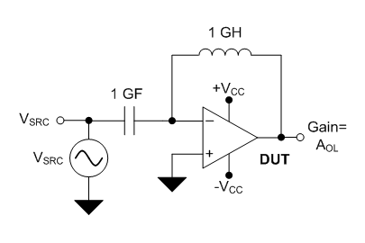
Figure 2: DUT configuration to determine AOL
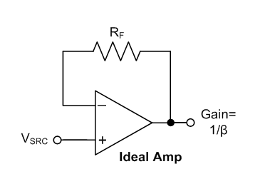
Figure 3: Ideal amplifier configuration to determine noise gain (1/β)
Figure 4 shows the simulated magnitude and phase of loop gain, AOL and 1/β. Since 1/β is purely resistive, its response is flat across frequency. The loop gain is AOL(dB) + β(dB) = AOL(dB), since the amplifier is in a unity-gain configuration as shown in Figure 3. The AOL and loop-gain curves thus lie on top of each other, as shown in Figure 4. Since this is a single-pole system, the total phase shift due to the AOL pole at fd is 90°. The resulting ΦM is thus 180°-90° = 90°, and the TIA is unconditionally stable.
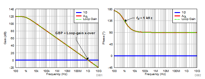
Figure 4: Simulated loop gain, AOL and 1/β for an ideal case
Effect of input capacitance (CTOT)
Let’s analyze the effect of capacitance at the amplifier’s inputs on loop-gain response. I’ll assume a total effective input capacitance, CTOT, of 10pF. The combination of CTOT and RF will create a zero in the 1/β curve at a frequency of fz = 1/(2πRFCTOT) = 100kHz. Figures 5 and 6 show the circuit and resulting frequency response. The AOL and 1/β curves intersect at 10MHz – the geometric mean of fz (100kHz) and the GBP (1GHz). A zero in the 1/β curve becomes a pole in the β curve. The resulting loop gain will have a two-pole response, as shown in Figure 6.
The zero causes the magnitude of 1/β to increase at 20dB/decade and intersect the AOL curve at a 40dB/decade rate of closure (ROC), resulting in potential instability. The dominant AOL pole at 1kHz results in a 90° phase shift in the loop gain. The zero frequency, fz, at 100kHz adds another 90° phase shift. Its effect is complete by 1MHz. Since the loop-gain crossover occurs at only 10MHz, the total phase shift from fd and fz will be 180°, resulting in ΦM = 0° and indicating that the TIA circuit is unstable.
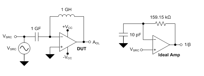
Figure 5: Simulation circuit including a 10pF input capacitor

Figure 6: Simulated loop gain, AOL and (1/β) when including the effects of input capacitance
Effect of feedback capacitance (CF)
To recover the phase loss due to fz, insert a pole, fp1, into the 1/β response by adding capacitor CF in parallel with RF. fp1 is located at 1/(2πRFCF). To get a maximally flat, closed-loop Butterworth response (ΦM = 64°), calculate CF using Equation 1:

where f-3dB is the closed-loop bandwidth shown in Equation 2:
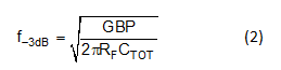
The calculated CF = 0.14pF and f-3dB = 10MHz. fz is located at ≈7MHz. The feedback capacitor includes the parasitic capacitances from the printed circuit board and RF. In order to minimize CPCB, remove the ground and power planes beneath the feedback trace between the amplifier’s inverting input and output pin. Using resistors with small form factors, such as 0201 and 0402 reduces parasitic capacitance caused by the feedback components. Figures 7 and 8 show the circuit and resulting frequency response.

Figure 7: Simulation circuit, including a 0.14pF feedback capacitor

Figure 8: Simulated loop gain, AOL and 1/β when including the effects of input and feedback capacitance
Using Bode-plot theory, Table 2 summarizes the points of inflection in the loop-gain response.

Table 2: Effect of poles and zeros on the loop-gain magnitude and phase
The 1/β curve reaches a maximum value of  . For a Butterworth response, 1/β intersects AOL near its maximum value at a frequency
  . fd and fz create a total phase shift of 180°. The phase reclaimed by fp1 is
  , which is very close to the simulated 65°.
When designing a TIA, you must know the photodiode’s capacitance, as this is usually fixed by the application. Given the photodiode capacitance, the next step is to select the correct amplifier for the application.
Choosing the right amplifier requires an understanding of the relationship between an amplifier’s GBP, the desired transimpedance gain and closed-loop bandwidth, and the input and feedback capacitances. You can find an Excel calculator incorporating the equations and theory described in this post here. If you are designing a TIA, be sure to check the calculator out. It will save you a lot of time and manual calculations.
Additional resources
- Download the application report, “Transimpedance Considerations for High-Speed Amplifiers,” for a quantitative derivation of Equations 1 and 2 in this post.
- Get online support in the TI E2E™ Community Amplifier forums.
- Browse more than 40 training videos on op-amp topics like noise, bandwidth and stability.
- Learn more about selecting the correct amplifier in the application note, “Transimpedance Amplifiers (TIA): Choosing the Best Amplifier for the Job.”
[转]What you need to know about transimpedance amplifiers – part 1的更多相关文章
- How to evaluate a transimpedance amplifier (part 2)
In my previous blog on "How to evaluate a transimpedance amplifier, part 1", we looked at ...
- How to evaluate a transimpedance amplifier (part 1)
In this blog, I want take a different approach and describe the technical challenge encountered whil ...
- DAC Essentials
http://e2e.ti.com/blogs_/b/analogwire/archive/tags/DAC%2bEssentials DAC Essentials: A new blog serie ...
- Connect to the DSP on C6A8168/DM8168/DM8148 using CCS
转自ti-wiki 这份wiki,我曾经就收藏过,但是没有加以重视,以至于绕了一大圈的ccs开发环境的配置,现在正式收藏于自己的博客中...总结良多啊 Connecting to DSP on C6 ...
- Operational Amplifiers
1>.Operational Amplifiers:different from the resistor,the inductor and the capacitor,it's a multi ...
- EEG montage
Source: WikiPedia - Electroencephalography Since an EEG voltage signal represents a difference betwe ...
- word20161201
http://baike.baidu.com/link?url=ZTTkA-suMlJNGb2AeNBE2E6MZQZwjkvWXKgmUpeLBIrCfC-k32cGJOJLrtDlLXjsTfkD ...
- tas5721 驱动
Submitter Mark Brown Date March 31, 2016, 5:33 p.m. Message ID <E1algTO-0004Cm-Ga@finisterre> ...
- AD8275 Driver Amplifiers For Analog-To-Digital Converters
Driver Amplifiers For Analog-To-Digital Converters What amplifiers are used to drive analog-to-digit ...
随机推荐
- memcached +php环境配置和分析
一.memcached 简介 在很多场合,我们都会听到 memcached 这个名字,但很多同学只是听过,并没有用过或实际了解过,只知道它是一个很不错的东东.这里简单介绍一下,memcached 是高 ...
- 《Focus On 3D Terrain Programming》中一段代码的注释二
取自<Focus On 3D Terrain Programming>中的一段: bool CTERRAIN::MakeTerrainFault( int iSize, int iIter ...
- ReportingService 通过RowNumber函数获取行号和生成隔行变色样式
以前一直没有搞明白SSRS里面的RowNumber函数到底该怎么用,所以一直没有很好的办法在SSRS中的表格上实现隔行变色的样式,实现隔行变色的关键就是获取表格中每一行的行号.在最近了解了下这个函数, ...
- Android开机自启动程序
背景知识:当Android启动时,会发出一个系统广播,内容为ACTION_BOOT_COMPLETED,它的字符串常量表示为 android.intent.action.BOOT_COMPLETED. ...
- 6*17点阵的Window程序, Java写的。
package com.wulala; import java.awt.BorderLayout;import java.awt.Color;import java.awt.Dimension;imp ...
- Server.MapPath()获取本机绝对路径
1. Server.MapPath("/") 应用程序根目录所在的位置 如 C:\Inetpub\wwwroot\ 2.Server.MapPath("./&qu ...
- JavaEE基础(七)
1.面向对象(构造方法Constructor概述和格式) A:构造方法概述和作用 给对象的数据(属性)进行初始化 B:构造方法格式特点 a:方法名与类名相同(大小也要与类名一致) b:没有返回值类型, ...
- 天大acm 题号1002 Maya Calendar
Description 上周末,M.A. Ya教授对古老的玛雅有了一个重大发现.从一个古老的节绳(玛雅人用于记事的工具)中,教授发现玛雅人使用了一个一年有365天的叫做Haab的历法.这 个Haab历 ...
- hdu4924 Football Manager
这题上来我是没有思路的.因为目标值关涉到的因素太多而直接枚举的复杂度又太高. 目标值由两部分合成,一部分是队员的CA和与PA和,另一部分是队员之间的relationship. 前者是简单的代数累加,而 ...
- 山东理工大学第七届ACM校赛-经济节约 分类: 比赛 2015-06-26 10:34 19人阅读 评论(0) 收藏
经济节约 Time Limit: 1000ms Memory limit: 65536K 有疑问?点这里^_^ 题目描述 由于经济紧张,某国国王决定减少一部分多余的士兵,这些士兵在边界都有各自的 ...