[转]What you need to know about transimpedance amplifiers – part 1
Transimpedance amplifiers (TIAs) act as front-end amplifiers for optical sensors such as photodiodes, converting the sensor’s output current to a voltage. TIAs are conceptually simple: a feedback resistor (RF) across an operational amplifier (op amp) converts the current (I) to a voltage (VOUT) using Ohm’s law, VOUT = I × RF. In this series of blog posts, I will show you how to compensate a TIA and optimize its noise performance. For a quantitative analysis of a TIA’s key parameters, such as bandwidth, stability and noise, please see the application note, ““Transimpedance Considerations for High-Speed Amplifiers.”
In a physical circuit, parasitic capacitances interact with the feedback resistor to create unwanted poles and zeros in the amplifier’s loop-gain response. The most common sources of parasitic input and feedback capacitances are the photodiode capacitance (CD), the op amp’s common-mode (CCM) and differential input capacitance (CDIFF), and the circuit-board capacitance (CPCB). The feedback resistor, RF is not ideal and has a parasitic shunt capacitance that may be as large as 0.2pF. In high-speed TIA applications, these parasitic capacitances interact with each other and RF to create a response that is not ideal. In this blog post, I will illustrate how to compensate a TIA.
Figure 1 shows a complete TIA circuit with parasitic-input and feedback-capacitance sources.

Figure 1: TIA circuit including parasitic capacitances
Three key factors determine the bandwidth of a TIA:
- Total input capacitance (CTOT).
- Desired transimpedance gain set by RF.
- The op amp’s gain-bandwidth product (GBP): the higher the gain bandwidth, the higher the resulting closed-loop transimpedance bandwidth.
These three factors are interrelated: for a particular op amp, targeting the gain will set the maximum bandwidth; conversely, targeting the bandwidth will set the maximum gain.
Single-pole amplifier with no parasitics
The first step of this analysis assumes an op amp with a single pole in the AOL response and the specifications shown in Table 1.

Table 1: TIA specifications
An amplifier’s closed-loop stability is related to its phase margin, ΦM, which is determined by the loop-gain response defined as AOL × β, where β is the inverse of the noise gain. Figures 2 and 3 show the TINA-TI™ circuits to determine the op amp’s AOL and noise gain, respectively. Figure 2 configures the device under test (DUT) in an open-loop configuration to derive its AOL. Figure 3 uses an ideal op amp with the desired RF, CF and CTOT around it to extract the noise gain, 1/β. Figure 3 excludes parasitic elements CF and CTOT – for now.
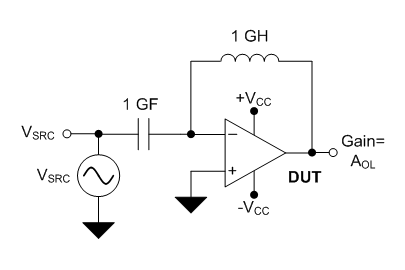
Figure 2: DUT configuration to determine AOL
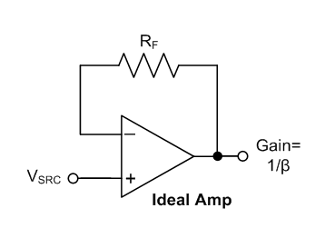
Figure 3: Ideal amplifier configuration to determine noise gain (1/β)
Figure 4 shows the simulated magnitude and phase of loop gain, AOL and 1/β. Since 1/β is purely resistive, its response is flat across frequency. The loop gain is AOL(dB) + β(dB) = AOL(dB), since the amplifier is in a unity-gain configuration as shown in Figure 3. The AOL and loop-gain curves thus lie on top of each other, as shown in Figure 4. Since this is a single-pole system, the total phase shift due to the AOL pole at fd is 90°. The resulting ΦM is thus 180°-90° = 90°, and the TIA is unconditionally stable.
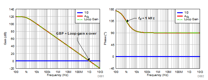
Figure 4: Simulated loop gain, AOL and 1/β for an ideal case
Effect of input capacitance (CTOT)
Let’s analyze the effect of capacitance at the amplifier’s inputs on loop-gain response. I’ll assume a total effective input capacitance, CTOT, of 10pF. The combination of CTOT and RF will create a zero in the 1/β curve at a frequency of fz = 1/(2πRFCTOT) = 100kHz. Figures 5 and 6 show the circuit and resulting frequency response. The AOL and 1/β curves intersect at 10MHz – the geometric mean of fz (100kHz) and the GBP (1GHz). A zero in the 1/β curve becomes a pole in the β curve. The resulting loop gain will have a two-pole response, as shown in Figure 6.
The zero causes the magnitude of 1/β to increase at 20dB/decade and intersect the AOL curve at a 40dB/decade rate of closure (ROC), resulting in potential instability. The dominant AOL pole at 1kHz results in a 90° phase shift in the loop gain. The zero frequency, fz, at 100kHz adds another 90° phase shift. Its effect is complete by 1MHz. Since the loop-gain crossover occurs at only 10MHz, the total phase shift from fd and fz will be 180°, resulting in ΦM = 0° and indicating that the TIA circuit is unstable.
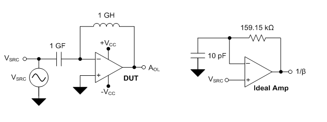
Figure 5: Simulation circuit including a 10pF input capacitor

Figure 6: Simulated loop gain, AOL and (1/β) when including the effects of input capacitance
Effect of feedback capacitance (CF)
To recover the phase loss due to fz, insert a pole, fp1, into the 1/β response by adding capacitor CF in parallel with RF. fp1 is located at 1/(2πRFCF). To get a maximally flat, closed-loop Butterworth response (ΦM = 64°), calculate CF using Equation 1:

where f-3dB is the closed-loop bandwidth shown in Equation 2:
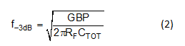
The calculated CF = 0.14pF and f-3dB = 10MHz. fz is located at ≈7MHz. The feedback capacitor includes the parasitic capacitances from the printed circuit board and RF. In order to minimize CPCB, remove the ground and power planes beneath the feedback trace between the amplifier’s inverting input and output pin. Using resistors with small form factors, such as 0201 and 0402 reduces parasitic capacitance caused by the feedback components. Figures 7 and 8 show the circuit and resulting frequency response.

Figure 7: Simulation circuit, including a 0.14pF feedback capacitor

Figure 8: Simulated loop gain, AOL and 1/β when including the effects of input and feedback capacitance
Using Bode-plot theory, Table 2 summarizes the points of inflection in the loop-gain response.

Table 2: Effect of poles and zeros on the loop-gain magnitude and phase
The 1/β curve reaches a maximum value of  . For a Butterworth response, 1/β intersects AOL near its maximum value at a frequency
 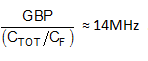 . fd and fz create a total phase shift of 180°. The phase reclaimed by fp1 is
  , which is very close to the simulated 65°.
When designing a TIA, you must know the photodiode’s capacitance, as this is usually fixed by the application. Given the photodiode capacitance, the next step is to select the correct amplifier for the application.
Choosing the right amplifier requires an understanding of the relationship between an amplifier’s GBP, the desired transimpedance gain and closed-loop bandwidth, and the input and feedback capacitances. You can find an Excel calculator incorporating the equations and theory described in this post here. If you are designing a TIA, be sure to check the calculator out. It will save you a lot of time and manual calculations.
Additional resources
- Download the application report, “Transimpedance Considerations for High-Speed Amplifiers,” for a quantitative derivation of Equations 1 and 2 in this post.
- Get online support in the TI E2E™ Community Amplifier forums.
- Browse more than 40 training videos on op-amp topics like noise, bandwidth and stability.
- Learn more about selecting the correct amplifier in the application note, “Transimpedance Amplifiers (TIA): Choosing the Best Amplifier for the Job.”
[转]What you need to know about transimpedance amplifiers – part 1的更多相关文章
- How to evaluate a transimpedance amplifier (part 2)
In my previous blog on "How to evaluate a transimpedance amplifier, part 1", we looked at ...
- How to evaluate a transimpedance amplifier (part 1)
In this blog, I want take a different approach and describe the technical challenge encountered whil ...
- DAC Essentials
http://e2e.ti.com/blogs_/b/analogwire/archive/tags/DAC%2bEssentials DAC Essentials: A new blog serie ...
- Connect to the DSP on C6A8168/DM8168/DM8148 using CCS
转自ti-wiki 这份wiki,我曾经就收藏过,但是没有加以重视,以至于绕了一大圈的ccs开发环境的配置,现在正式收藏于自己的博客中...总结良多啊 Connecting to DSP on C6 ...
- Operational Amplifiers
1>.Operational Amplifiers:different from the resistor,the inductor and the capacitor,it's a multi ...
- EEG montage
Source: WikiPedia - Electroencephalography Since an EEG voltage signal represents a difference betwe ...
- word20161201
http://baike.baidu.com/link?url=ZTTkA-suMlJNGb2AeNBE2E6MZQZwjkvWXKgmUpeLBIrCfC-k32cGJOJLrtDlLXjsTfkD ...
- tas5721 驱动
Submitter Mark Brown Date March 31, 2016, 5:33 p.m. Message ID <E1algTO-0004Cm-Ga@finisterre> ...
- AD8275 Driver Amplifiers For Analog-To-Digital Converters
Driver Amplifiers For Analog-To-Digital Converters What amplifiers are used to drive analog-to-digit ...
随机推荐
- C语言初学者代码中的常见错误与瑕疵(9)
题目 字母的个数 现在给你一个由小写字母组成字符串,要你找出字符串中出现次数最多的字母,如果出现次数最多字母有多个那么输出最小的那个. 输入:第一行输入一个正整数T(0<T<25) 随后T ...
- scala匿名函数
package com.ming.test import scala.math._ object AnonymousFunc { def valueAtOneQuarter(f:(Double)=&g ...
- HTML5与移动端Web
概述 HTML5 提供了很多新的功能,主要有: 新的 HTML 元素,例如 section, nav, header, footer, article 等 用于绘画的 Canvas 元素 用于多媒体播 ...
- Mysql String Functions
SUBSTRING_INDEX(str,delim,count) 按标识符截取指定长度的字符串 mysql); -> 'www.mysql' mysql); -> 'mysql.com' ...
- Nagios监控Oralce
一.本文说明: 本文是监控本地的Oracle,其实监控远端的Oracle也是跟下面的步骤差不多的. 二.安装Nagios.Nagios插件.NRPE软件: 安装步骤可以参考<Linux下Nagi ...
- 在centos6.5-64bit上安装wxHexEditor,以查看编译二进制文件
目前在做一个存储,磁盘里面的数据老是出现很诡异的地方,某个通道的录像播放到一半的时候,切换到另外一个通道的视频上去了,一直不知道怎么下手,想着用十六进制编辑器查看磁盘数据. sudo yum inst ...
- SQLServer学习笔记<> 表连接查询----交叉连接、内连接、左连接、右连接
(1)交叉连接(cross join)即我们所说的笛卡尔积.查询出满足两张表所有的记录数,A(3条记录),B(9条记录),A*B(27条记录). 比如:雇员表(HR.employees)和货运公司(S ...
- CSS select样式列表-------美化列表
<!DOCTYPE html PUBLIC "-//W3C//DTD XHTML 1.0 Transitional//EN" "http://www.w3.org/ ...
- Session案例:简易的购物车
三个jsp和两个Servlet组成:在WebContent下边建立一个shoppingcart文件夹,将三个jsp文件放在里面: 1.建立一个step1.jsp文件,出现一个表格,是一个复选框,可以选 ...
- 20150625_Andriod_01_ListView1_条目选中
android listview 参考地址: http://www.cnblogs.com/zhengbeibei/archive/2013/05/14/3078805.html http://xy ...