
STM32F4 -- How to use the DMA burst feature
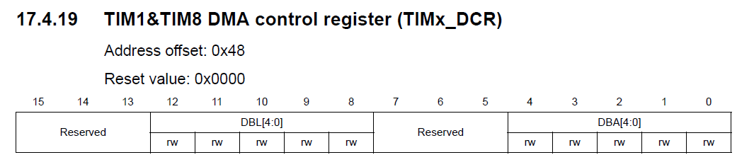
Bits 15:13 Reserved, must be kept at reset value.
Bits 12:8 DBL[4:0]: DMA burst length
This 5-bit vector defines the number of DMA transfers
(the timer detects a burst transfer when a read or a write access to the TIMx_DMAR register address is performed).
- 00000: 1 transfer
- 00001: 2 transfers
- 00010: 3 transfers
- ...
- 10001: 18 transfers
Bits 7:5 Reserved, must be kept at reset value.
Bits 4:0 DBA[4:0]: DMA base address
This 5-bits vector defines the base-address for DMA transfers (when read/write access are done through the TIMx_DMAR address).
DBA is defined as an offset starting from the address of the TIMx_CR1 register.
Example:
- 00000: TIMx_CR1,
- 00001: TIMx_CR2,
- 00010: TIMx_SMCR,
...

Example: Let us consider the following transfer: DBL = 7 transfers and DBA = TIMx_CR1.
In this case the transfer is done to/from 7 registers starting from the TIMx_CR1 address.

Bits 15:0 DMAB[15:0]: DMA register for burst accesses
A read or write operation to the DMAR register accesses the register located at the address
(TIMx_CR1 address) + (DBA + DMA index) x 4
DBA is defined as an offset starting from the address of the TIMx_CR1 register.
where TIMx_CR1 address is the address of the control register 1,
DBA is the DMA base address configured in TIMx_DCR register,
DMA index is automatically controlled by the DMA transfer,
and ranges from 0 to DBL (DBL configured in TIMx_DCR).
DBL This 5-bit vector defines the number of DMA transfers
Example of how to use the DMA burst feature
In this example the timer DMA burst feature is used to update the contents of the CCRx registers (x = 2, 3, 4)
with the DMA transferring half words into the CCRx registers.
This is done in the following steps:
1. Configure the corresponding DMA channel as follows:
– DMA channel peripheral address is the DMAR register address
– DMA channel memory address is the address of the buffer in the RAM
containing the data to be transferred by DMA into CCRx registers.
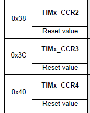
– Number of data to transfer = 3 (See note below).: CCR2, CCR3, CCR4
– Circular mode disabled.
2. Configure the DCR register by configuring the DBA and DBL bit fields as follows:
DBL = 3 transfers, DBA = 0xE. :: 4 * 0x0E = 0x38
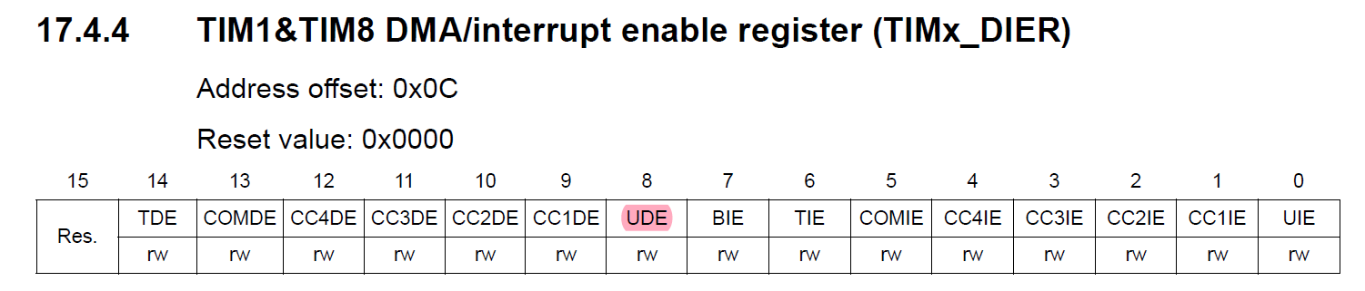
3. Enable the TIMx update DMA request (set the UDE bit in the DIER register).
4. Enable TIMx
5. Enable the DMA channel
Note:
This example is for the case where every CCRx register to be updated once.
Let's take the example of a buffer in the RAM containing data1, data2, data3.
The data is transferred to the CCRx registers as follows:
on the update DMA request, data1 is transferred to CCR2, data2 is transferred to CCR3, data3 is transferred to CCR4 and
If every CCRx register is to be updated twice for example, the number of data to transfer should be 6 -- DMA
NumberOfTransfer = UpdateTimes * DMA burst length<DBL>.
Let's take the example of a buffer in the RAM containing data1, data2, data3, data4, data5 and data6.
The data is transferred to the CCRx registers as follows:
on the first update DMA request, data1 is transferred to CCR2, data2 is transferred to CCR3, data3 is transferred to CCR4 and
on the second update DMA request, data4 is transferred to CCR2, data5 is transferred to CCR3 and data6 is transferred to CCR4.
/**
******************************************************************************
* @file TIM/TIM_DMABurst/main.c
* @author MCD Application Team
* @version V1.1.0
* @date 18-January-2013
* @brief Main program body
******************************************************************************
* @attention
*
* <h2><center>© COPYRIGHT 2013 STMicroelectronics</center></h2>
*
* Licensed under MCD-ST Liberty SW License Agreement V2, (the "License");
* You may not use this file except in compliance with the License.
* You may obtain a copy of the License at:
*
* http://www.st.com/software_license_agreement_liberty_v2
*
* Unless required by applicable law or agreed to in writing, software
* distributed under the License is distributed on an "AS IS" BASIS,
* WITHOUT WARRANTIES OR CONDITIONS OF ANY KIND, either express or implied.
* See the License for the specific language governing permissions and
* limitations under the License.
*
******************************************************************************
*/ /* Includes ------------------------------------------------------------------*/
#include "main.h" /** @addtogroup STM32F4xx_StdPeriph_Examples
* @{
*/ /** @addtogroup TIM_DMABurst
* @{
*/ /* Private typedef -----------------------------------------------------------*/
/* Private define ------------------------------------------------------------*/
#define TIM1_DMAR_ADDRESS ((uint32_t)0x4001004C) /* TIM DMAR address */ /* Private macro -------------------------------------------------------------*/
/* Private variables ---------------------------------------------------------*/
GPIO_InitTypeDef GPIO_InitStructure;
DMA_InitTypeDef DMA_InitStructure;
TIM_TimeBaseInitTypeDef TIM_TimeBaseStructure;
TIM_OCInitTypeDef TIM_OCInitStructure; uint16_t aSRC_Buffer[] = {0x0FFF, 0x0000, 0x0555}; // APR, RCR, CCR1 /* Private function prototypes -----------------------------------------------*/
static void TIM_Config(void); /* Private functions ---------------------------------------------------------*/ /**
* @brief Main program
* @param None
* @retval None
*/
int main(void)
{
/*!< At this stage the microcontroller clock setting is already configured,
this is done through SystemInit() function which is called from startup
files (startup_stm32f40xx.s/startup_stm32f427x.s) before to branch to
application main.
To reconfigure the default setting of SystemInit() function, refer to
system_stm32f4xx.c file
*/ /* TIM1 Configuration */
TIM_Config(); /* Time base configuration */
/* -----------------------------------------------------------------------
TIM1 Configuration: generate 1 PWM signal using the DMA burst mode: TIM1 input clock (TIM1CLK) is set to 2 * APB2 clock (PCLK2), since APB2 prescaler is different from 1.
TIM1CLK = 2 * PCLK2, PCLK2 = HCLK / 2 => TIM1CLK = 2 * (HCLK / 2) = HCLK = SystemCoreClock To get TIM1 counter clock at 24 MHz, the prescaler is computed as follows:
Prescaler = (TIM1CLK / TIM1 counter clock) - 1
Prescaler = (SystemCoreClock /24 MHz) - 1 The TIM1 period is 5.8 KHz:
TIM1 Frequency = TIM1 counter clock/(ARR + 1) = 24 MHz / 4096 = 5.85 KHz
TIM1 Channel1 duty cycle = (TIM1_CCR1/ TIM1_ARR)* 100 = 33.33% Note:
SystemCoreClock variable holds HCLK frequency and is defined in system_stm32f4xx.c file.
Each time the core clock (HCLK) changes, user had to call SystemCoreClockUpdate()
function to update SystemCoreClock variable value. Otherwise, any configuration
based on this variable will be incorrect.
----------------------------------------------------------------------- */
TIM_TimeBaseStructure.TIM_Period = 0xFFFF;
TIM_TimeBaseStructure.TIM_Prescaler = (uint16_t) (SystemCoreClock / ) - ;
TIM_TimeBaseStructure.TIM_ClockDivision = 0x0;
TIM_TimeBaseStructure.TIM_CounterMode = TIM_CounterMode_Up;
TIM_TimeBaseInit(TIM1, &TIM_TimeBaseStructure); /* TIM Configuration in PWM Mode */
TIM_OCInitStructure.TIM_OCMode = TIM_OCMode_PWM1;
TIM_OCInitStructure.TIM_OutputState = TIM_OutputState_Enable;
TIM_OCInitStructure.TIM_Pulse = 0xFFF;
TIM_OC1Init(TIM1, &TIM_OCInitStructure); /* TIM1 DMAR Base register and DMA Burst Length Config */
TIM_DMAConfig(TIM1, TIM_DMABase_ARR, TIM_DMABurstLength_3Transfers); // APR, RCR, CCR1 /* TIM1 DMA Update enable */
TIM_DMACmd(TIM1, TIM_DMA_Update, ENABLE); /* TIM1 enable */
TIM_Cmd(TIM1, ENABLE); /* TIM1 PWM Outputs Enable */
TIM_CtrlPWMOutputs(TIM1, ENABLE); /* Enable DMA2 Stream5 */
DMA_Cmd(DMA2_Stream5, ENABLE); /* Wait until DMA2 Stream5 end of Transfer */
while (!DMA_GetFlagStatus(DMA2_Stream5, DMA_FLAG_TCIF5))
{
} /* Infinite loop */
while()
{
}
} /**
* @brief Configure the TIM1 Pins.
* @param None
* @retval None
*/
static void TIM_Config(void)
{
GPIO_InitTypeDef GPIO_InitStructure; /* TIM1 clock enable */
RCC_APB2PeriphClockCmd(RCC_APB2Periph_TIM1, ENABLE); /* GPIOA clock enable */
RCC_AHB1PeriphClockCmd(RCC_AHB1Periph_GPIOA, ENABLE); /* DMA2 clock enable */
RCC_AHB1PeriphClockCmd(RCC_AHB1Periph_DMA2, ENABLE); /* GPIOA Configuration: PA8(TIM1 CH1) as alternate function push-pull */
GPIO_InitStructure.GPIO_Pin = GPIO_Pin_8;
GPIO_InitStructure.GPIO_Mode = GPIO_Mode_AF;
GPIO_InitStructure.GPIO_Speed = GPIO_Speed_100MHz;
GPIO_InitStructure.GPIO_OType = GPIO_OType_PP;
GPIO_InitStructure.GPIO_PuPd = GPIO_PuPd_NOPULL;
GPIO_Init(GPIOA, &GPIO_InitStructure); /* Connect TIM pins to AF1 */
GPIO_PinAFConfig(GPIOA, GPIO_PinSource8, GPIO_AF_TIM1); /* DeInitialize the DMA2 Stream5 */
DMA_DeInit(DMA2_Stream5); DMA_InitStructure.DMA_Channel = DMA_Channel_6; // TIM1_UP : DMA2_Stream5
DMA_InitStructure.DMA_PeripheralBaseAddr = (uint32_t)TIM1_DMAR_ADDRESS;
DMA_InitStructure.DMA_Memory0BaseAddr = (uint32_t)aSRC_Buffer;
DMA_InitStructure.DMA_DIR = DMA_DIR_MemoryToPeripheral;
DMA_InitStructure.DMA_BufferSize = ;
DMA_InitStructure.DMA_PeripheralInc = DMA_PeripheralInc_Disable;
DMA_InitStructure.DMA_MemoryInc = DMA_MemoryInc_Enable;
DMA_InitStructure.DMA_PeripheralDataSize = DMA_PeripheralDataSize_HalfWord;
DMA_InitStructure.DMA_MemoryDataSize = DMA_MemoryDataSize_HalfWord;
DMA_InitStructure.DMA_Mode = DMA_Mode_Normal;
DMA_InitStructure.DMA_Priority = DMA_Priority_VeryHigh;
DMA_InitStructure.DMA_FIFOMode = DMA_FIFOMode_Enable;
DMA_InitStructure.DMA_FIFOThreshold = DMA_FIFOThreshold_Full;
DMA_InitStructure.DMA_MemoryBurst = DMA_MemoryBurst_Single;
DMA_InitStructure.DMA_PeripheralBurst = DMA_PeripheralBurst_Single;
DMA_Init(DMA2_Stream5, &DMA_InitStructure);
} #ifdef USE_FULL_ASSERT /**
* @brief Reports the name of the source file and the source line number
* where the assert_param error has occurred.
* @param file: pointer to the source file name
* @param line: assert_param error line source number
* @retval None
*/
void assert_failed(uint8_t* file, uint32_t line)
{
/* User can add his own implementation to report the file name and line number,
ex: printf("Wrong parameters value: file %s on line %d\r\n", file, line) */ while ()
{}
}
#endif /**
* @}
*/ /**
* @}
*/ /************************ (C) COPYRIGHT STMicroelectronics *****END OF FILE****/
STM32F4 -- How to use the DMA burst feature的更多相关文章
- PCI总线 DMA burst 基本概念
转载地址:http://blog.csdn.net/sunjiajiang/article/details/7945057 DMA和burst不是一个概念. DMA传送不经过CPU的控制,假如硬盘的数 ...
- 嵌入式开发之hi3519---PCIE DMA
http://blog.csdn.net/abcamus/article/details/76167747 大话pcie dma http://blog.csdn.net/qingfengtsing/ ...
- LCD framebuffer驱动设计文档
内容提要:1. android display相关的名词2. 调试LCD驱动需要注意的步骤3. 关于帧缓冲区及I/O内存---------------------------------------- ...
- stm32之内部功能
本文将提到以下内容: 位带操作 中断 printf重定向 随机数发生器RNG AD/DA DMA 高性能计算能力 加密 ART加速 一.位带操作 在学习51单片机的时候就使用过位操作,通过关键字sbi ...
- s3c2410 cs8900a 网卡驱动程序
/* CS8900a.h */ #define CONFIG_CERF_CS8900A 1 /* * cs8900a.c: A Crystal Semiconductor (Now Cirrus Lo ...
- [转]理解下DMA/NorFlash/DDR下的Burst是个什么概念
DMA传送不经过CPU的控制,假如硬盘的数据不能经过DMA控制器读到内存,那么每完成一次将硬盘的数据读出来,再存放到内存的操作,都要通过CPU运行几条读写指令来完成,这时CPU就做不了别的事了,如果有 ...
- STM32F4 SPI with DMA
STM32F4 SPI with DMA A few people have requested code, so I thought I’d post the code showing how I’ ...
- stm32f4 dma + uart idle + double 调试小记
使用 stm32f4 调试uart 接收, 使用 空闲中断,dma 双缓冲模式,有以下几点需要注意的. 调试的时候断点不要打在 if (USART_GetITStatus(USART6, USART_ ...
- STM32 F4 DAC DMA Waveform Generator
STM32 F4 DAC DMA Waveform Generator Goal: generating an arbitrary periodic waveform using a DAC with ...
随机推荐
- python中的__getattr__、__getattribute__、__setattr__、__delattr__、__dir__
__getattr__: 属性查找失败后,解释器会调用 __getattr__ 方法. class TmpTest: def __init__(self): self.tmp = 'tmp12 ...
- 第5月第13天 node cnpm安装 babel
1. https://nodejs.org/en/download/ http://www.runoob.com/react/react-install.html 2. npm install --s ...
- GDB命令
recursiveDescription 打印view层次结构
- linux系统下如何批量更改文件夹里面所有相同字符【转】
如网上源码下载下来我们需要调试,调试过程中需要修改里面相同文字,下面提供三种方法供参考 通过sed命令替换 sed -i "s/oldyunwei/newyunwei/g" gre ...
- 一步步实现windows版ijkplayer系列文章之一——Windows10平台编译ffmpeg 4.0.2,生成ffplay
一步步实现windows版ijkplayer系列文章之一--Windows10平台编译ffmpeg 4.0.2,生成ffplay 一步步实现windows版ijkplayer系列文章之二--Ijkpl ...
- 010_MAC下权限问题的那些事
一. arun:bin arunyang$ sh catalina.sh start #启动tomcat报一堆的没有权限~~~~(>_<)~~~~ 二.解决如下 aru ...
- poj1273
赤裸裸的最大流 #include <iostream> #include <cstdio> #include <cstdlib> #include <cstr ...
- 用Fiddler对Android应用进行抓包
前言 Fiddler是一款非常流行并且实用的http抓包工具,它的原理是在本机开启了一个http的代理服务器,然后它会转发所有的http请求和响应,因此,它比一般的firebug或者是chrome自带 ...
- Git(四)Git的分支管理
一. 创建合并分支原理 在我们每次的提交,Git都把它们串成一条时间线,这条时间线就是一个分支.截止到目前,只有一条时间线,在Git里,这个分支叫主分支,即master分支.HEAD指针严格来说不是指 ...
- 插件bootstrap-table
基于Metronic的Bootstrap开发框架经验总结(16)-- 使用插件bootstrap-table实现表格记录的查询.分页.排序等处理 在业务系统开发中,对表格记录的查询.分页.排序等处理是 ...