
STM32F4 SPI with DMA
STM32F4 SPI with DMA
A few people have requested code, so I thought I’d post the code showing how I’ve configured my GPIO, timer, SPI, DMA and NVIC modules, along with some explanation of how the system works.
Note that I’m using the STM32F4 Standard Peripheral Libraries.
The first step is to enable clock signals to the required modules via the RCC (Reset and Clock Control) module:
RCC
//Configure the clocks for the required modules
//Enable GPIO peripheral clocks
RCC_AHB1PeriphClockCmd(RCC_AHB1Periph_GPIOA, ENABLE);
RCC_AHB1PeriphClockCmd(RCC_AHB1Periph_GPIOB, ENABLE);
RCC_AHB1PeriphClockCmd(RCC_AHB1Periph_GPIOC, ENABLE);
RCC_AHB1PeriphClockCmd(RCC_AHB1Periph_GPIOD, ENABLE);//Enable the Serial Peripheral Interface peripheral clocks
RCC_APB1PeriphClockCmd(RCC_APB1Periph_SPI2, ENABLE);//Enable the Direct Memory Access peripheral clocks
RCC_AHB1PeriphClockCmd(RCC_AHB1Periph_DMA1, ENABLE);//Enable the timer peripheral clocks
RCC_APB1PeriphClockCmd(RCC_APB1Periph_TIM3, ENABLE);
RCC_APB1PeriphClockCmd(RCC_APB1Periph_TIM4, ENABLE);
GPIO
#define GPIO_SCAN_PORT GPIOB
#define GPIO_SCAN_PIN GPIO_Pin_7
#define GPIO_XLAT_PORT GPIOA
#define GPIO_XLAT_PIN GPIO_Pin_5
#define GPIO_BLANK_PORT GPIOB
#define GPIO_BLANK_PIN GPIO_Pin_6
//Configure the GPIO Pins
GPIO_InitTypeDef GPIO_InitStructure;//Timer3&4 Outputs (TLC5940 GSCLK and BLANK)
GPIO_InitStructure.GPIO_Pin = (GPIO_Pin_4 | GPIO_Pin_6);
GPIO_InitStructure.GPIO_Mode = GPIO_Mode_AF;
GPIO_InitStructure.GPIO_OType = GPIO_OType_PP;
GPIO_InitStructure.GPIO_Speed = GPIO_Speed_100MHz;
GPIO_InitStructure.GPIO_PuPd = GPIO_PuPd_NOPULL;
GPIO_Init(GPIOB, &GPIO_InitStructure);
//Connect Timers to the GPIO Pins
GPIO_PinAFConfig(GPIOB, GPIO_PinSource4, GPIO_AF_TIM3); //Connect TIM3 OC1 output to PortB Pin4 (GSCLK)
GPIO_PinAFConfig(GPIOB, GPIO_PinSource6, GPIO_AF_TIM4); //Connect TIM4 OC1 output to PortB Pin6 (BLANK)//TLC5940 XLAT Pin
GPIO_InitStructure.GPIO_Pin = GPIO_XLAT_PIN;
GPIO_InitStructure.GPIO_Mode = GPIO_Mode_OUT;
GPIO_InitStructure.GPIO_OType = GPIO_OType_PP;
GPIO_InitStructure.GPIO_Speed = GPIO_Speed_100MHz;
GPIO_InitStructure.GPIO_PuPd = GPIO_PuPd_NOPULL;
GPIO_Init(GPIO_XLAT_PORT, &GPIO_InitStructure);//Display SCAN Pin
GPIO_InitStructure.GPIO_Pin = GPIO_SCAN_PIN;
GPIO_InitStructure.GPIO_Mode = GPIO_Mode_OUT;
GPIO_InitStructure.GPIO_OType = GPIO_OType_PP;
GPIO_InitStructure.GPIO_Speed = GPIO_Speed_100MHz;
GPIO_InitStructure.GPIO_PuPd = GPIO_PuPd_NOPULL;
GPIO_Init(GPIO_SCAN_PORT, &GPIO_InitStructure);//SPI2 Pins
// SCLK = PB10
// NSS = PB9
GPIO_InitStructure.GPIO_Pin = GPIO_Pin_9 | GPIO_Pin_10;
GPIO_InitStructure.GPIO_Mode = GPIO_Mode_AF;
GPIO_InitStructure.GPIO_OType = GPIO_OType_PP;
GPIO_InitStructure.GPIO_Speed = GPIO_Speed_50MHz;
GPIO_InitStructure.GPIO_PuPd = GPIO_PuPd_NOPULL;
GPIO_Init(GPIOB, &GPIO_InitStructure);
GPIO_PinAFConfig(GPIOB, GPIO_PinSource9, GPIO_AF_SPI2);
GPIO_PinAFConfig(GPIOB, GPIO_PinSource10, GPIO_AF_SPI2);// MISO = PC2
// MOSI = PC3
GPIO_InitStructure.GPIO_Pin = GPIO_Pin_2 | GPIO_Pin_3;
GPIO_Init(GPIOC, &GPIO_InitStructure);
GPIO_PinAFConfig(GPIOC, GPIO_PinSource2, GPIO_AF_SPI2);
GPIO_PinAFConfig(GPIOC, GPIO_PinSource3, GPIO_AF_SPI2);
The main points of interest here are that I’m connecting TIM3’s OC1 output directly to a GPIO pin for GSCLK, and TIM4’s OC1 output for the BLANK signal.
SPI
//Initialise the SPI module
SPI_InitTypeDef SPI_InitStructure;
SPI_InitStructure.SPI_Direction = SPI_Direction_2Lines_FullDuplex; //The SPI bus setup uses two lines, one for Rx and one for Tx
SPI_InitStructure.SPI_Mode = SPI_Mode_Master; //STM32 is the master with the TLC5940s as slaves
SPI_InitStructure.SPI_DataSize = SPI_DataSize_8b; //Use 8-bit data transfers
SPI_InitStructure.SPI_CPOL = SPI_CPOL_Low; //TLC5940 clock is low when idle
SPI_InitStructure.SPI_CPHA = SPI_CPHA_1Edge; //TLC5940 uses first clock transition as the "capturing edge"
SPI_InitStructure.SPI_NSS = SPI_NSS_Soft; //Software slave-select operation
SPI_InitStructure.SPI_BaudRatePrescaler = SPI_BaudRatePrescaler_8; //Set the prescaler
SPI_InitStructure.SPI_FirstBit = SPI_FirstBit_MSB; //TLC5940 data is transferred MSB first
SPI_InitStructure.SPI_CRCPolynomial = 0; //No CRC used
SPI_Init(SPI2, &SPI_InitStructure); //Initialise the SPI2 peripheral
SPI_SSOutputCmd(SPI2, ENABLE); //Set the SS Pin as an Output (master mode)
SPI_Cmd(SPI2, ENABLE);
My choice of SPI clock prescaler is fairly arbitrary, but the key points here are that I’ve configured the clock phase and polarity
as per the TLC5940 datasheet, and all transfers will be 8bits (more on this later).
DMA
DMA module for SPI transfers is as follows:
//Initialise the DMA1 Stream 4 Channel 0 for SPI2_TX DMA access#define DISP_SCAN_DATA_CNT (24 * 3 * 2) //24 bytes per chip, one chip per colour (RGB), two boards
volatile uint8_t dispData0[DISP_SCAN_DATA_CNT];
volatile uint8_t dispData1[DISP_SCAN_DATA_CNT];DMA_InitTypeDef DMA_InitStructure;
DMA_InitStructure.DMA_Channel = DMA_Channel_0; //SPI2 Tx DMA is DMA1/Stream4/Channel0
DMA_InitStructure.DMA_PeripheralBaseAddr = (uint32_t)&(SPI2->DR); //Set the SPI2 Tx
DMA_InitStructure.DMA_Memory0BaseAddr = (uint32_t)&dispData0; //Set the memory location
DMA_InitStructure.DMA_DIR = DMA_DIR_MemoryToPeripheral; //Sending data from memory to the peripheral's Tx register
DMA_InitStructure.DMA_BufferSize = DISP_SCAN_DATA_CNT; //Define the number of bytes to send
DMA_InitStructure.DMA_PeripheralInc = DMA_PeripheralInc_Disable; //Don't increment the peripheral 'memory'
DMA_InitStructure.DMA_MemoryInc = DMA_MemoryInc_Enable; //Increment the memory location
DMA_InitStructure.DMA_PeripheralDataSize = DMA_PeripheralDataSize_Byte; //Byte size memory transfers
DMA_InitStructure.DMA_MemoryDataSize = DMA_MemoryDataSize_Byte; //Byte size memory transfers
DMA_InitStructure.DMA_Mode = DMA_Mode_Normal; //Normal mode (not circular)
DMA_InitStructure.DMA_Priority = DMA_Priority_High; //Priority is high to avoid saturating the FIFO since we are in direct mode
DMA_InitStructure.DMA_FIFOMode = DMA_FIFOMode_Disable; //Operate in 'direct mode' without FIFO
DMA_Init(DMA1_Stream4, &DMA_InitStructure);//Enable the transfer complete interrupt for DMA1 Stream4
DMA_ITConfig(DMA1_Stream4, DMA_IT_TC, ENABLE); //Enable the Transfer Complete interrupt
This is a memory to peripheral (SPI module) transfer, sending DISP_SCAN_DATA_CNT (24 * 3 * 2 = 144) bytes per transfer.
The memory address is incremented after every byte, and the Transfer Complete flag generates an interrupt.
NVIC
Next, I’ve configured the NVIC (Nested Vectored Interrupt Controller) for two interrupt service routine triggers:
//Initialise the Nested Vectored Interrupt Controller
NVIC_InitTypeDef NVIC_InitStructure;//Enable the TIM4 (BLANK) Interrupt
NVIC_InitStructure.NVIC_IRQChannel = TIM4_IRQn;
NVIC_InitStructure.NVIC_IRQChannelPreemptionPriority = 0;
NVIC_InitStructure.NVIC_IRQChannelSubPriority = 0;
NVIC_InitStructure.NVIC_IRQChannelCmd = ENABLE;
NVIC_Init(&NVIC_InitStructure);//Enable the DMA1 Stream4 (SPI2_TX) Interrupt
NVIC_InitStructure.NVIC_IRQChannel = DMA1_Stream4_IRQn;
NVIC_InitStructure.NVIC_IRQChannelPreemptionPriority = 0;
NVIC_InitStructure.NVIC_IRQChannelSubPriority = 1;
NVIC_InitStructure.NVIC_IRQChannelCmd = ENABLE;
NVIC_Init(&NVIC_InitStructure);
The BLANK interrupt is used for generating the BLANK pulse, initialising DMA transfers, and latching previously transferred data after each SCAN cycle.
Timers
Finally, the timer modules are configured:
#define TLC5940_GSCLK_COUNTS 256 //GSCLK Counts between BLANK Pulses
#define TLC5940_GSCLK_FREQ 1000000 //GSCLK Frequency
#define TLC5940_BLANK_COUNT 50 //Padding to allow previous SCAN column’s positive supply rail to turn off before switching to the next column
#define TIM_APB1_FREQ 84000000 //Internal TIMx Clock frequency (CK_INT)
//Initalise the Timer Modules
TIM_TimeBaseInitTypeDef TIM_BaseInitStructure;
TIM_OCInitTypeDef TIM_OCInitStructure;//Deinitialise timer modules and the initialisation structures
TIM_DeInit(TIM3);
TIM_DeInit(TIM4);
TIM_TimeBaseStructInit(&TIM_BaseInitStructure);
TIM_OCStructInit(&TIM_OCInitStructure);//Setup the TIM3 to generate the 'master clock'
TIM_BaseInitStructure.TIM_Period = 1;
TIM_BaseInitStructure.TIM_Prescaler = (uint16_t) (((TIM_APB1_FREQ / TLC5940_GSCLK_FREQ)/4) - 1); //Note that the division factor of 4 is due to the OC1 freq vs CK_INT freq
TIM_BaseInitStructure.TIM_ClockDivision = TIM_CKD_DIV1;
TIM_BaseInitStructure.TIM_CounterMode = TIM_CounterMode_Up;
TIM_TimeBaseInit(TIM3, &TIM_BaseInitStructure);
//Configure Channel 1 Output Compare as the Trigger Output (used to generate the 'GSCLK' signal)
TIM_OCInitStructure.TIM_OCMode = TIM_OCMode_Toggle;
TIM_OCInitStructure.TIM_OutputState = TIM_OutputState_Enable;
TIM_OCInitStructure.TIM_Pulse = 1;
TIM_OCInitStructure.TIM_OCPolarity = TIM_OCPolarity_High;
TIM_OC1Init(TIM3, &TIM_OCInitStructure);
TIM_OC1PreloadConfig(TIM3, TIM_OCPreload_Enable);//Setup the TIM4 base for a symmetrical counter with a maximum count specified as the 'GSCLK count' (effectively the TLC5940's greyscale resolution)
TIM_BaseInitStructure.TIM_Period = TLC5940_GSCLK_COUNTS + TLC5940_BLANK_COUNT; //GSCLK overflow count (with 1 extra for the BLANK signal to 'block')
TIM_BaseInitStructure.TIM_Prescaler = 0;
TIM_BaseInitStructure.TIM_ClockDivision = TIM_CKD_DIV1;
TIM_BaseInitStructure.TIM_CounterMode = TIM_CounterMode_CenterAligned1;
TIM_TimeBaseInit(TIM4, &TIM_BaseInitStructure);
//Configure Channel 1 Output Compare as the Trigger Output (used as the clock signal by TIM4 to generate 'BLANK' pulses)
TIM_OCInitStructure.TIM_OCMode = TIM_OCMode_PWM1;
TIM_OCInitStructure.TIM_OutputState = TIM_OutputState_Enable;
TIM_OCInitStructure.TIM_Pulse = TLC5940_BLANK_COUNT;
TIM_OCInitStructure.TIM_OCPolarity = TIM_OCPolarity_High;
TIM_OC1Init(TIM4, &TIM_OCInitStructure);
TIM_OC1PreloadConfig(TIM4, TIM_OCPreload_Enable);//Configure TIM3 as a master timer
TIM_SelectOutputTrigger(TIM3, TIM_TRGOSource_Update); //TRGO is tied to the update of TIM3
TIM_SelectMasterSlaveMode(TIM3, TIM_MasterSlaveMode_Enable); //TIM3 enabled as a master//Configure TIM4 as a slave
TIM_SelectInputTrigger(TIM4, TIM_TS_ITR2); //Set TIM4 (slave) to trigger off TIM3 (master)
TIM_SelectSlaveMode(TIM4, TIM_SlaveMode_External1); //Use the master signal input as an 'external clock'//Configure the TIM4 module to interrupt at Capture/Compare 1 events (match on both up and down-counting)
TIM_ITConfig(TIM4, TIM_IT_CC1, ENABLE);
//Enable Timers 3 and 4
TIM_Cmd(TIM4, ENABLE);
TIM_Cmd(TIM3, ENABLE);
Here, Timer 3 is used as the master clock, generating the GSCLK signal on its Output Compare 1 line, and driving Timer 4 which is configured as a centre-aligned PWM output on OC1.
Blank count is effectively a padded pulse, allowing for:
- Minimum BLANK pulse time
- XLAT and DMA transfer triggering
- The MOSFET output on the previous SCAN column to fully discharge (I’ve tuned this by viewing discharge time on my oscilloscope)
The GSCLK frequency is set, and the number of GSCLK pulses between falling and rising BLANK signal edges is set to 256 since I’m using 8-bit colour rather than the full capability of the TLC5940 chip (12-bit). This means that there will be 256 GSCLK cycles between BLANK pulses.
The peripherals are now fully configured, so the last thing to do is look at the interrupt service routines, and investigate the results:
ISRs
#define DISP_SCAN_FREQ 200 //Frequency of the SCAN signal
#define DISP_BLANK_CYCLE_LIMIT ((((TLC5940_GSCLK_FREQ / (TLC5940_GSCLK_COUNTS + TLC5940_BLANK_COUNT)) / DISP_SCAN_FREQ) / 2) - 1) //Number of BLANK cycles to count before SCANing
void TIM4_IRQHandler(void)
{
//TIM4 IRQ Handler has several tasks:
// - Toggles the SCAN signal
// - Latches the previously transmitted data for the newly selected ('scanned') column
// - Sets up and starts the SPI2 DMA Stream to transmit the next column's data
//All this should be performed within the window of the BLANK signal (TIM4 OC1) being high (not the full SPI transmission)//Check if the interrupt generated is an OC1 Update
if(TIM_GetFlagStatus(TIM4,TIM_IT_CC1))
{
//Clear the TIM4 CC1 interrupt bit
TIM_ClearITPendingBit(TIM4, TIM_IT_CC1);//Only perform event when down-counting (this ensures the XLAT pulse, SCAN update, and SPI transfers are triggered within the BLANK pulse)
if(TIM4->CR1 & TIM_CR1_DIR)
{
//Check if we require a 'SCAN' update (XLAT pulse, SCAN toggle, and next transfer triggered)
if(dispBlankCycleCnt++ >= DISP_BLANK_CYCLE_LIMIT)
{
GPIO_SetBits(GPIO_XLAT_PORT, GPIO_XLAT_PIN); //Set the XLAT pin
dispBlankCycleCnt = 0; //Reset the counter//Determine the current column, and shift accordingly
if(dispCurrentCol)
{
dispCurrentCol = 0; //Change to column '0'
GPIO_SetBits(GPIO_SCAN_PORT, GPIO_SCAN_PIN); //Set the SCAN pin (note that column 0 is a logic high, column 1 is a logic low)
DMA1_Stream4->M0AR = (uint32_t)&dispData1; //Send *next* column's data (dispData1 is sent (for the next cycle) since the current column is now '0')
}
else
{
dispCurrentCol = 1; //Change to column '1'
GPIO_ResetBits(GPIO_SCAN_PORT, GPIO_SCAN_PIN); //Reset the SCAN pin (note that column 0 is a logic high, column 1 is a logic low)
DMA1_Stream4->M0AR = (uint32_t)&dispData0; //Send *next* column's data (dispData0 is sent (for the next cycle) since the current column is now '1')
}GPIO_ResetBits(GPIO_XLAT_PORT, GPIO_XLAT_PIN); //Clear the XLAT pin
//Trigger the next transfer
SPI_I2S_DMACmd(SPI2, SPI_I2S_DMAReq_Tx, ENABLE); //Enable the DMA Transmit Request
DMA_Cmd(DMA1_Stream4, ENABLE); //Enable the DMA stream assigned to SPI2
}
}
}
}void DMA1_Stream4_IRQHandler(void)
{
//Check if the transfer complete interrupt flag has been set
if(DMA_GetITStatus(DMA1_Stream4, DMA_IT_TCIF4) == SET)
{
//Clear the DMA1 Stream4 Transfer Complete flag
DMA_ClearITPendingBit(DMA1_Stream4, DMA_IT_TCIF4);
}
}
The DMA ISR is currently not used (I do intend to use it for something unrelated), but the TIM4 ISR essentially controls the whole of the display.
The rising edge of the BLANK pulse (effectively) triggers the interrupt. After determining that the correct ISR triggered the event, the TIM_CR1_DIR bit is used to check if the counter is down-counting. This ensures that we only perform the following tasks at the rising edge of the BLANK pulse.
Every time the ISR is run, we increment a counter and if this counter exceeds the number required to SCAN the display, we latch the previous data using the XLAT signal, toggle the SCAN signal, and transfer the next data (found in the dispData0[ ] or dispData1[ ] arrays.
The number of BLANK cycles to wait before SCANning is calculated in DISP_BLANK_CYCLE_LIMIT, which takes into account:
- TLC5940_GSCLK_FREQ – Greyscale clock frequency
- TLC5940_GSCLK_COUNTS + TLC5940_BLANK_COUNT – The number of GSCLK pulses between rising BLANK edges
- DISP_SCAN_FREQ – The frequency we would like to SCAN the array at (set to 200Hz here)
Updating the data in the dispDatax[ ] arrays will now change what is displayed on the LEDs.
With a GSCLK frequency of 1MHz and a SCAN frequency of 200Hz, I have no noticeable LED flicker even though I’ve heard people talk about using >5MHz to avoid it with their setups.
Logic Analysis
I’ve attached a logic analyser between the STM32F407 outputs and the TLC5940 display-board input and this is what appears:
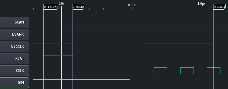
Now that we know the GSCLK period is as expected, we can investigate the BLANK time to determine the greyscale data is being clocked for 8-bit resolution.
The time between the falling and rising BLANK edges is 305.6 – 49.6 = 256us which is as expected.
I’ve also investigated on a closer level to check the phase of the signals are correct for 2^8 counts.
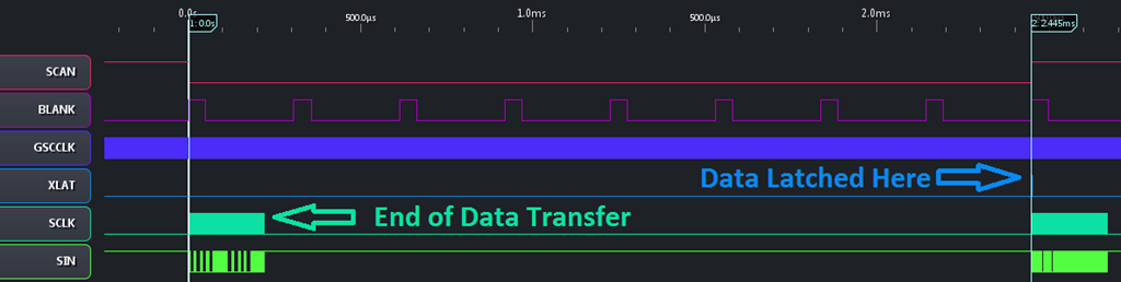
Finally, checking the scan width, we can see that one column is enabled for 2.445ms.
This means that the SCAN rate is 409Hz; fairly good considering 2.5us = is not evenly divisible by 256us.
The capture above also shows that when the BLANK count reaches the limit, the associated ISR latches the previous data,
toggles the SCAN line, and then triggers the SPI transfer.
It then counts the required number of BLANK cycles before latching this data (XLAT signal barely visible to the right of the blue arrow where the 2,445ms cursor is).
Feel free to comment on the above, and let me know if anything is unclear.
STM32F4 SPI with DMA的更多相关文章
- STM32F4 SPI双机通讯调试总结
1.如果查询方式进行数据收发,不管是Master,还是Slave,流程如下:(假设收发n+1个字节) a.等待TXE,写入一个字节 b.等待TXE,写入一个字节 c.等待RXNE,读取一个字节 循环b ...
- STM32的SPI口的DMA读写[原创www.cnblogs.com/helesheng]
SPI是我最常用的接口之一,连接管脚仅为4根:在常见的芯片间通信方式中,速度远优于UART.I2C等其他接口.STM32的SPI口的同步时钟最快可到PCLK的二分之一,单个字节或字的通信时间都在us以 ...
- SPI中的极性CPOL和相位CPHA
详解SPI中的极性CPOL和相位CPHA SPI由于接口相对简单(只需要4根线),用途算是比较广泛,主要应用在 EEPROM,FLASH, 实时时钟,AD转换器,还有数字信号处理器和数字信号解码器之间 ...
- SPI接口的FLASH
SPI flash W25Qxx: W25Q系列的spiflash.每页(Page)256B,每16个page为一个sector(扇区=4KB),每16个扇区为一个block(块=64KB) W25Q ...
- (stm32学习总结)—spi基本原理
参考:spi详解 spi协议 SPI的基本介绍 SPI的简介 SPI,是英语Serial Peripheral interface的缩写,顾名思义就是串行外围设备接口,是Motorola首先在其M ...
- stm32 DAC输出音频
#define DAC_DHR8R1_Address 0x40007410 // Init Structure definition DAC_InitTypeDef DAC_InitStructure ...
- STM32F030系列实现仿位带操作
1.闲言 最近开发的时候,用到了STM32F030F4P6型号的单片机,它只有20个引脚,价格非常便宜,但是功能齐全:定时器.外部中断.串口.IIC.SPI.DMA和WWDG等等,应用尽有,非常适合用 ...
- 【安富莱STM32H7教程】第1章 初学STM32H7的准备工作
完整教程下载地址:http://forum.armfly.com/forum.php?mod=viewthread&tid=86980 第1章 初学STM32H7的准备工作 俗话说万事开头 ...
- STM32F030-UART1_DMA使用提示
STM32F030-UART1_DMA使用提示 前言: 今天把STM32F030C8T6的串口DMA学习了一下,为了加快各位研发人员的开发进度,避免浪费大量的时间在硬件平台上,写出个人代码调试的经验. ...
随机推荐
- Linux - sed 文本操作
SED 是一项Linux指令,功能同awk类似,差别在于,sed简单,对列处理的功能要差一些,awk的功能复杂,对列处理的功能比较强大. sed全称是:Stream EDitor 调用sed命令有两种 ...
- PHP-Redis操作
/*1.Connection*/ $redis = new Redis(); $redis->connect('127.0.0.1',6379,1);//短链接,本地host,端口为6379,超 ...
- C# 常用控件属性及方法介绍
C#常用控件属性及方法介绍 目录 1.窗体(Form) 2.Label (标签)控件 3.TextBox ...
- HDU 6406 Taotao Picks Apples 线段树维护
题意:给个T,T组数据: 每组给个n,m:n个数,m个操作: (对序列的操作是,一开始假设你手上东西是-INF,到i=1时拿起1,之后遍历,遇到比手头上的数量大的数时替换(拿到手的算拿走),问最后拿走 ...
- 全国大学API接口分享
1.获取省份列表: http://119.29.166.254:9090/api/provinces 返回的是省份列表,其中id很重要. 2.通过省份id查询省份城市: http://119.29.1 ...
- 记一次HashMap面试
记一次HashMap面试 从网上已经身边同事朋友的面试情况来看,面试HashMap几乎是必问的,网上也很多类似的文章,但是真面起来,发现还是有很多点可以深抠的.本篇就结合一次面试经历说一下之前没有注意 ...
- ESXi 6.5 总是会话超时
ESXi 6.5 客户端Web界面会话超时 在VMware ESXi 6.5中,主机客户端Web界面会话每15分钟自动超时一次,然后您必须再次重新登录ESXi主机客户端Web界面. 要避免这种繁琐的情 ...
- 奈奎斯特定理 and 香农定理
-----------------------整理自<21ic电子网> 奈奎斯特定理(Nyquist's Theorem)和香农定理(Shannon's Theorem)是网络传输中的两个 ...
- TP-Link wr703N 使用华为HiLink系列上网卡的设置【转】
转自:http://www.right.com.cn/forum/thread-103082-1-1.html 最近买了一个华为的E303s的上网卡,之前703的openwrt是按照需要拨号和使用U盘 ...
- ajax请求成功但不执行success-function回调函数的问题
在success:function(data){}下面加个error:function(){},看看是不是出错了走了error.如果是,说明返回值类型不符合要求. 比如:下面代码返回String类型. ...