基于SILVACO ATLAS的a-IGZO薄膜晶体管二维器件仿真(01)
最近因为肺炎的缘故,宅在家里不能出门,就翻了下一些资料,刚好研究方向是这个,就简单研究了下。参考资料主要如下:
1.《半导体工艺和器件仿真软件Silvaco TCAD实用教程》 唐龙谷 2014
2.《长安大学 半导体工艺与器件仿真指导书》 张林 2015
引用本科时社团一姐的一句话:学习PS的精髓在于毁图。个人浅见,学习仿真的话还是要根据实例拆解分析比较快。重复,我是新手,只是个人浅见。
官网实例:https://www.silvaco.com/examples/tcad/section41/index.html
tftex10.in : Amorphous IGZO TFT Simulation:
# (c) Silvaco Inc., 2019
# This example demonstrates simulation of amorphous IGZO (indium galium
# zinc oxide) TFT. Here we reproduce the results from:
#
# Fung, T., Chuang, C., Chen, C., Katsumi, A., Cottle, R., Townsend, M.,
# Kumomi, H., and Kanicki, J., "Two-dimensional numerical simulation of
# radio frequency sputter amorphous In-Ga-Zn-O thin-film transistors",
# J. Appl. Phys., V. 106, pp. 084511-1 through 084511-10.
#
# Comparisons with experiment are included.
#
# This first part of the input deck simulates Id-Vg.
#
go atlas mesh width=180 outf=tftex10_1.str master.out x.m l=0 s=0.25
x.m l=40 s=0.25
y.m l=0 s=0.0005
y.m l=0.02 s=0.0005
y.m l=0.12 s=0.005
#(划分网格)
# The device is composed of a 20 nm layer of IGZO deposited
# 100 nm oxide on a n++ substrate that acts as the gate.
#
region num=1 material=igzo y.min=0 y.max=0.02
region num=2 material=sio2 y.min=0.02 y.max=0.12
#(定义材料)
elec num=1 name=gate bottom
elec num=2 name=source y.max=0.0 x.min=0.0 x.max=5.0
elec num=3 name=drain y.max=0.0 x.min=35.0 x.max=40.0
#(定义电极)
# We define the gate as N.POLY. This pins the gate workfunction
# to the conduction band edge of silicon.
#
contact num=1 n.poly
#
# We also define a workfunction for the source and drain that
# is very close to the conduction edge. In the reference the
# authors observed that without a workfunction the results for
# ohmic boundaries were not significantly different than the
# Schottky model.
#
contact num=2 workf=4.33
contact num=3 workf=4.33
#(定义接触条件)
models fermi
#
# Key to the characterization of amorphous materials is the
# definition of the states within the band gap.
#
defects nta=1.55e20 ntd=1.55e20 wta=0.013 wtd=0.12 \
nga=0.0 ngd=6.5e16 egd=2.9 wgd=0.1 \
sigtae=1e-15 sigtah=1e-15 sigtde=1e-15 sigtdh=1e-15 \
siggae=1e-15 siggah=1e-15 siggde=1e-15 siggdh=1e-15 \
dfile=tftex10_don.dat afile=tftex10_acc.dat numa=128 numd=64
#(定义缺陷分布)
# From here we simply extract the Id-Vg characteristic
#
solve init
solve prev
#???
solve vdrain=0.1
save outf=tftex10_0.str
log outf=tftex10_1a.log
solve vgate=0 vstep=-0.1 vfinal=-5 name=gate log off
#???
load inf=tftex10_0.str master
solve prev
log outf=tftex10_1b.log
solve vstep=0.2 vfinal=20.0 name=gate
#
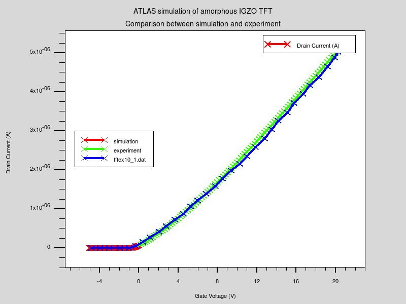
# And we compare the simulation with experimental data reported in
# the reference.
#
tonyplot -overlay tftex10_1a.log tftex10_1b.log tftex10_1.dat -set tftex10_1.set
#tonyplot 的 overlay与set命令 ???
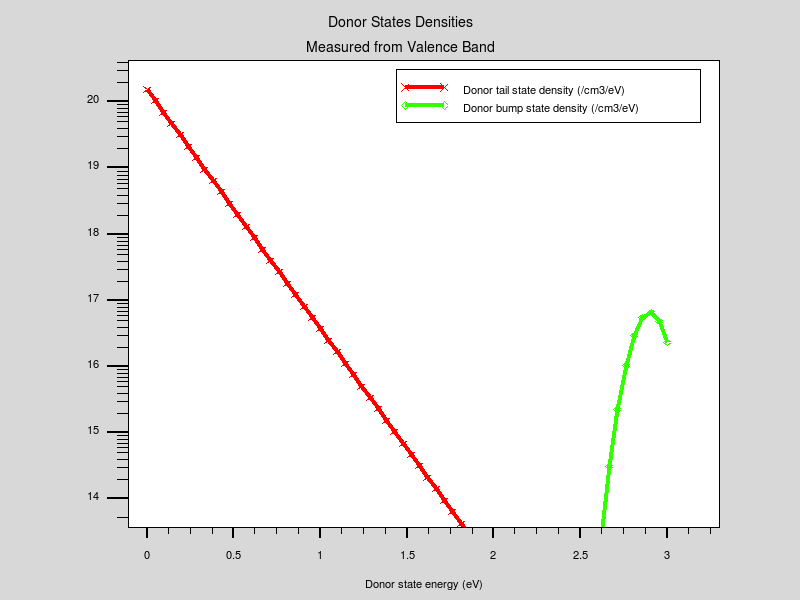
tonyplot -overlay tftex10_don.dat -set tftex10_don.set
#绘制施主态密度分布曲线
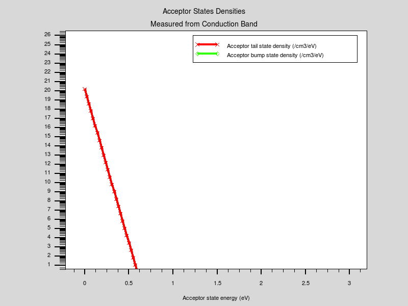
tonyplot -overlay tftex10_acc.dat -set tftex10_acc.set
#绘制受主态密度分布曲线 go atlas
#
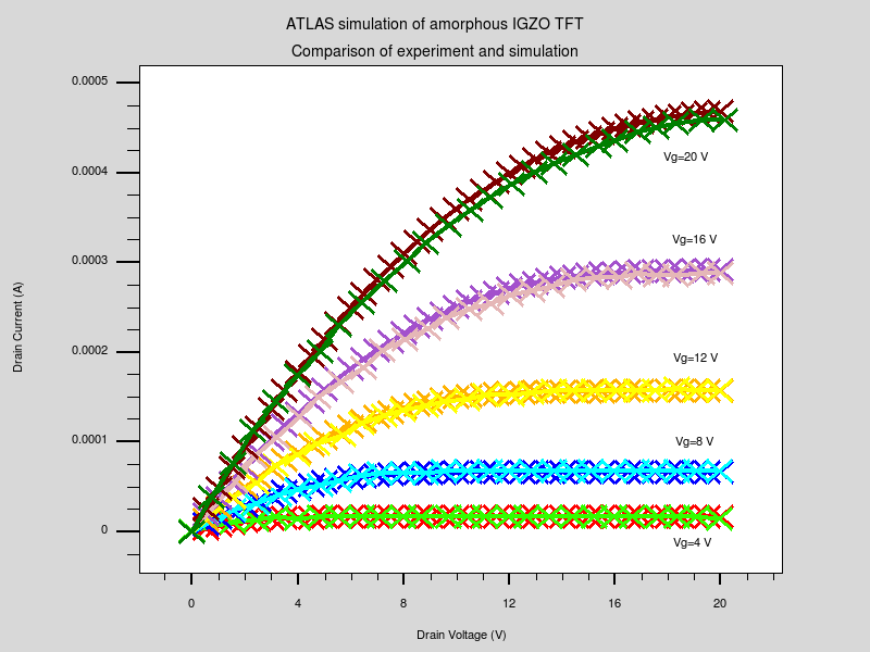
# In the next part of the input deck we extract the Id-Vd family of
# curves. The structure definition is exactly the same.
#
mesh width=180 x.m l=0 s=0.25
x.m l=40 s=0.25
y.m l=0 s=0.0005
y.m l=0.02 s=0.0005
y.m l=0.12 s=0.005 region num=1 material=igzo y.min=0 y.max=0.02
region num=2 material=sio2 y.min=0.02 y.max=0.12 elec num=1 name=gate bottom
elec num=2 name=source y.max=0.0 x.min=0.0 x.max=5.0
elec num=3 name=drain y.max=0.0 x.min=35.0 x.max=40.0 contact num=1 n.poly
contact num=2 workf=4.33
contact num=3 workf=4.33 models fermi defects nta=1.55e20 ntd=1.55e20 wta=0.013 wtd=0.12 \
nga=0.0 ngd=6.5e16 egd=2.9 wgd=0.1 \
sigtae=1e-15 sigtah=1e-15 sigtde=1e-15 sigtdh=1e-15 \
siggae=1e-15 siggah=1e-15 siggde=1e-15 siggdh=1e-15 \
dfile=don afile=acc numa=128 numd=64
#
# Here we calculate the start structures for each of the IdVd
# family by performing an initial gate ramp.
#
#(下面就有点懵了...)
solve solve vstep=0.2 vfinal=4.0 name=gate save outf=tftex10_2.str
solve vstep=0.2 vfinal=8.0 name=gate save outf=tftex10_3.str
solve vstep=0.2 vfinal=12.0 name=gate save outf=tftex10_4.str
solve vstep=0.2 vfinal=16.0 name=gate save outf=tftex10_5.str
solve vstep=0.2 vfinal=20.0 name=gate save outf=tftex10_6.str

load inf=tftex10_2.str master log outf=tftex10_2.log
solve vdrain=0.0 vstep=0.5 vfinal=20.0 name=drain

load inf=tftex10_3.str master log outf=tftex10_3.log
solve vdrain=0.0 vstep=0.5 vfinal=20.0 name=drain

load inf=tftex10_4.str master log outf=tftex10_4.log
solve vdrain=0.0 vstep=0.5 vfinal=20.0 name=drain

load inf=tftex10_5.str master log outf=tftex10_5.log
solve vdrain=0.0 vstep=0.5 vfinal=20.0 name=drain

load inf=tftex10_6.str master log outf=tftex10_6.log
solve vdrain=0.0 vstep=0.5 vfinal=20.0 name=drain

tonyplot -overlay tftex10_2.log tftex10_2.dat tftex10_3.log tftex10_3.dat tftex10_4.log tftex10_4.dat tftex10_5.log tftex10_5.dat tftex10_6.log tftex10_6.dat -set tftex10_2.set

quit
官网给出的四张输出图像如下:
自己装的ATLAS还有点问题,这几天先折腾下在跑跑看。
不过毕竟是引用了别人的文献中的数据,与实验室的材料特性还有较大差距,估计要手调了。
总体来说,ATLAS的步骤主要为:
建立网格-定义材料-定义电极以及接触-定义缺陷分布或掺杂-引入模型以及求解方法-求解-Tonyplot输出
要解决的难点主要在于:
1.材料特性微调;
2.缺陷分布调整;
3.理解输出语句,并合理运用;
武汉加油!
基于SILVACO ATLAS的a-IGZO薄膜晶体管二维器件仿真(01)的更多相关文章
- 基于SILVACO ATLAS的a-IGZO薄膜晶体管二维器件仿真(03)
今天逛ResearchGate的时候发现了一个不错的Atlas入门教程:Step by step with ATLAS Silvaco点击链接免费下载.. Atlas代码结构 当然可能有一点太基础了. ...
- 基于SILVACO ATLAS的a-IGZO薄膜晶体管二维器件仿真(08)
进展比较慢啊... 根据江南大学硕士论文IGZO/IZO双有源层薄膜晶体管特性的模拟研究: 其中, gCBa:类受主导带尾态 gVBd:类施主价带尾态 gGd:类施主氧空位态 NDeep:价带尾深施主 ...
- 基于SILVACO ATLAS的a-IGZO薄膜晶体管二维器件仿真(02)
Silvaco的破解用了好久好久,而且之后拷了上次例子的代码,Tonyplot的输出存在报错,还是四连. 当然这个点一下还是会出图的.但是,源代码稍微改了下结构,又有报错,而且程序直接终止. go a ...
- 基于SILVACO ATLAS的a-IGZO薄膜晶体管二维器件仿真(06)
在知网看到了江南大学的硕士论文: 双有源层a-IGZO薄膜晶体管的特性仿真 IGZO/IZO双有源层薄膜晶体管特性的模拟研究 发现,我昨天的文章中参数的设置存在重大失误,如下材料定义语句中: mate ...
- 基于SILVACO ATLAS的a-IGZO薄膜晶体管二维器件仿真(04)
在eetop上有好多好东西啊: Silvaco_TCAD_中文教程1 不过这个教程里是Linux系统的,而且工艺仿真占了比较大的篇幅. defect region=1 nta=5e17 wta=0.1 ...
- 基于SILVACO ATLAS的a-IGZO薄膜晶体管二维器件仿真(07)
今天主要解决一下defect语句: defect region=1 nta=1.55e20 wta=0.013 wtd=0.12 ngd=6.5e16 wga=2 ntd=1.55e20 ngd=0 ...
- 基于SILVACO ATLAS的a-IGZO薄膜晶体管二维器件仿真(05)
关于特性曲线的输出调整: 初代版本 material material=igzo eg300=3.5 nc300=8.5e21 nv300=8.5e21 taun0=1e-9 taup0=1e-9 a ...
- 基于SignalR的消息推送与二维码描登录实现
1 概要说明 使用微信扫描登录相信大家都不会陌生吧,二维码与手机结合产生了不同应用场景,基于二维码的应用更是比较广泛.为了满足ios.android客户端与web短信平台的结合,特开发了基于Singl ...
- 在云平台上基于Go语言+Google图表API提供二维码生成应用
二维码能够说已经深深的融入了我们的生活其中.到处可见它的身影:但通常我们都是去扫二维码, 曾经我们分享给朋友一个网址直接把Url发过去,如今我们能够把自己的信息生成二维码再分享给他人. 这里就分享一下 ...
随机推荐
- 数据库中的sql语句总结
初识SQL 1. 什么是SQL:结构化查询语言(Structured Query Language). 2. SQL的作用:客户端使用SQL来操作服务器. > 启动mysql.exe,连 ...
- 树莓派3b 换国内源 更新源
在国内要更新源的时候,因为是国外的源,总会出现网速太慢的问题, 以下是对于安装了,2017-11-29-raspbian-stretch 系统源 更换最好用root登陆操作 sudo passwd r ...
- Python之旅第五天(习题集合)
4天时间,虽然上着班,但是学的东西还是有点多,而且晚上看的比较容易忘,所以今天是习题模式,正好教程也是这么要求的,本来以为时间不长,没想到还是很崩溃啊.不多说,上干货. #关于随机产生验证码同时验证用 ...
- pandas玩转excel-> (1)如何利用pandas创建【行,列,单元格】
import pandas as pd #------新建单元格的方法一:通过先创建字典的形式 #可以先新建一个字典d={'x':100,'y':200,'z':300} #打印字典的索引print( ...
- spark之RDD练习
目录 一.基础练习 练习一:翻倍列表中的数值并排序列表,并选出其中大于等于10的元素. 练习二:将字符数组里面的每一个元素先切分在压平. 练习三:求两个列表中的交集.并集.及去重后的结果 练习四:对L ...
- Docker最全教程——从理论到实战(二十)
前言 各种编程语言均有其优势和生态,有兴趣的朋友完全可以涉猎多门语言.在平常的工作之中,也可以尝试选择相对适合的编程语言来完成相关的工作. 在团队技术文档站搭建这块,笔者尝试了许多框架,最终还是选择了 ...
- CSS隐藏元素的五种方法
1.opacity:0 2.visibility:hidden 3.diaplay:none 4.position:absolute display display属性依照词义真正隐藏元素.将disp ...
- ps导出svg
svg初识 看到一些复杂的svg图形很好奇是手写出来的么,看了源码望而却步.网上看到ps都可以导出svg,然后试了下. 需要加载一个脚本,js写的,把文件复制到路径后重启ps,修改图形名字,然后保存成 ...
- css动画延迟好像有点怪
项目中需要使用到动画animate.css,在自定义的时候发现设置animation-delay 和 animation-duration 的总时间不对会导致 动画缺失. 比如 bounceInLef ...
- POJ 2096 Collecting Bugs (概率DP,求期望)
Ivan is fond of collecting. Unlike other people who collect post stamps, coins or other material stu ...