MAX II Device Compatibility with 5.0-V CMOS Devices
http://www.altera.com/literature/hb/max2/max2_mii51009.pdf
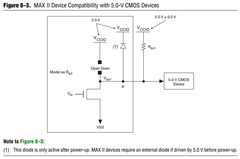
The open-drain pin never drives high, only low or tri-state. When the open-drain pin is active, it drives low.
When the open-drain pin is inactive, the pin is tri-stated and the trace pulls up to 5.0 V by the external resistor.
The purpose of enabling the I/O clamp diode is to protect the MAX II device’s I/O pins.
The 3.3-V VCCIO supplied to the I/O clamp diodes causes the voltage at point A to clamp at 4.0 V,
which meets the MAX II device’s reliability limits when the trace voltage exceeds 4.0 V.
The device operates successfully because a 5.0-V input is within its input specification.
The I/O clamp diode is only supported in the EPM1270 and EPM2210 devices’ I/O Bank 3.
An external protection diode is needed for other I/O banks in EPM1270 and EPM2210 devices
and all I/O pins in EPM240 and EPM570 devices.
The pull-up resistor value should be small enough for sufficient signal rise time,
but large enough so that it does not violate the IOL (output low) specification of MAX II devices.
The maximum MAX II device IOL depends on the programmable drive strength of the I/O output.
Table 8–1 shows the programmable drive strength settings
that are available for the 3.3-V LVTTL/LVCMOS I/O standard for MAX II devices.
The Quartus II software uses the maximum current strength as the default setting.
The PCI I/O standard is always set at 20 mA with no alternate setting.

To compute the required value of REXT, first calculate the model of the open-drain
transistors on the MAX II device. This output resistor (REXT) can be modeled by
dividing VOL by IOL (REXT = VOL/IOL). Table 8–2 shows the maximum VOL for the 3.3-V
LVTTL/LVCMOS I/O standard for MAX II devices.
f For more information about I/O standard specifications, refer to the DC and Switching
Characteristics chapter in the MAX II Device Handbook.

Select REXT so that the MAX II device’s IOL specification is not violated. You can
compute the required pull-up resistor value of REXT by using the equation: REXT =
(VCC/IOL) – RINT. For example, if an I/O pin is configured as a 3.3-V LVTTL with a 16
mA drive strength, given that the maximum power supply (VCC) is 5.5 V, the value of
REXT can be calculated as follows:

This resistor value computation assumes worst-case conditions. You can adjust the
REXT value according to the device configuration drive strength. Additionally, if your
system does not see a wide variation in voltage-supply levels, you can adjust these
calculations accordingly.
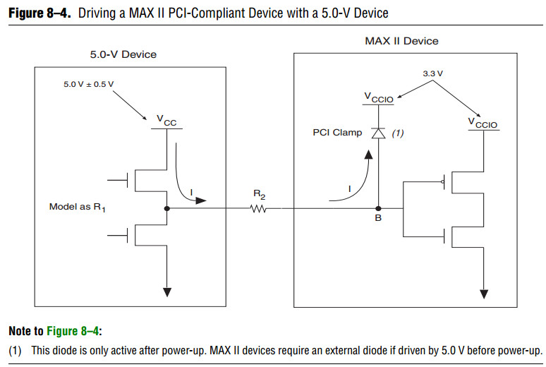
Because MAX II devices are 3.3-V, 32-bit, 66-MHz PCI compliant, the input circuitry
accepts a maximum high-level input voltage (VIH) of 4.0 V.
To drive a MAX II device with a 5.0-V device, you must connect a resistor (R2)
between the MAX II device and the 5.0-V device. See Figure 8–4.
If VCCIO for MAX II devices is 3.3 V and the I/O clamp diode is enabled, the voltage at point B in Figure 8–4 is 4.0 V,
which meets the MAX II devices reliability limits when the trace voltage exceeds 4.0 V.
To limit large current draw from the 5.0-V device, R2 should be small enough for a fast signal rise time
and large enough so that it does not violate the high-level output current (IOH) specifications of the devices driving the trace.
To compute the required value of R2, first calculate the model of the pull-up transistors on the 5.0-V device.
This output resistor (R1) can be modeled by dividing the 5.0-V device supply voltage (VCC) by the IOH: R1 = VCC/IOH
Figure 8–5 shows an example of typical output drive characteristics of a 5.0-V device.
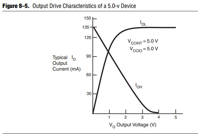
As shown above, R1 = 5.0 V/135 mA.
The values usually shown in data sheets reflect typical operating conditions.
Subtract 20% from the data sheet value for guard band.
This subtraction applied to the above example gives R1 a value of 30.
Select R2 so that the MAX II device’s IOH specification is not violated. For example,
if the above device has a maximum IOH of 8 mA, given the I/O clamp diode,
VIN = VCCIO + 0.7 V = 3.7 V.
Given that the maximum supply load of a 5.0-V device (VCC) is 5.5 V, the value of R2
can be calculated as follows:

This analysis assumes worst-case conditions. If your system does not see a wide
variation in voltage-supply levels, you can adjust these calculations accordingly.
Because 5.0-V device tolerance in MAX II devices requires use of the I/O clamp, and
this clamp is activated only after power-up, 5.0-V signals may not be driven into the
device until it is configured.
The I/O clamp diode is only supported in the EPM1270 and EPM2210 devices’ I/O Bank 3.
An external protection diode is needed for other I/O banks for EPM1270 and EPM2210 devices
and all I/O pins in EPM240 and EPM570 devices.
MAX II Device Compatibility with 5.0-V CMOS Devices的更多相关文章
- Multiplexing SDIO Devices Using MAX II or CoolRunner-II CPLD
XAPP906 Supporting Multiple SD Devices with CoolRunner-II CPLDs There has been an increasing demand ...
- Delphi XE5 Device compatibility
Delphi XE5 Device compatibility https://docs.google.com/spreadsheet/ccc?key=0AoEN2CEsVvJ0dGhVaWJE ...
- 3、一、Introduction(入门):2、Device Compatibility(设备兼容性)
2.Device Compatibility(设备兼容性) Android is designed to run on many different types of devices, from ...
- java.lang.UnsatisfiedLinkError: org.apache.hadoop.util.NativeCrc32.nativeComputeChunkedSumsByteArray(II[BI[BIILjava/lang/String;JZ)V
环境: Spark2.1.0 .Hadoop-2.7.5 代码运行系统:Win 7在运行Spark程序写出文件(savaAsTextFile)的时候,我遇到了这个错误: // :: ERROR U ...
- Android Google官方文档解析之——Device Compatibility
Android is designed to run on many different types of devices, from phones to tablets and television ...
- win7上代码连接hadoop出现错误 :org.apache.hadoop.util.NativeCrc32.nativeComputeChunkedSumsByteArray(II[BI[BIILjava/lang/String;JZ)V
在idea和eclipse中调试hadoop中hdfs文件,之前好好的,结果突然就出现java.lang.UnsatisfiedLinkError: org.apache.hadoop.util.Na ...
- 关于freemarker标签+Spring3.0 V层学习
import标签 就是把其他的ftl页面引用进来 <#import "/common/ui.ftl" as ui> 使用时 <@ui.message/>,m ...
- linux内核挂载根文件系统时报错”VFS: Cannot open root device "ram0" or unknown-block(0,0): error -6“如何处理?
1. 通过error -6得到: #define ENXIO 6 /* No such device or address */ 2. 解决办法 使能CONFIG_BL ...
- VFS: Cannot open root device "nfs" or unknown-block(0,255)错误的解决
1. 解决办法:在内核配置时候文件系统中选中Root file system on NFS
随机推荐
- android设备休眠
从上面的连接里面找到了一些资料: 如果一开始就对Android手机的硬件架构有一定的了解,设计出的应用程序通常不会成为待机电池杀手,而要设计出正确的通信机制与通信协议也并不困难.但如果不去了解而盲目设 ...
- 分别使用docx4j,jacob将文字与图片插入word中书签位置
项目中需要将一段文字,与人员的签名(图片)插入到上传的word中,上网查询了一下,有许多种方式可以向word中插入文字,发现docx4j与jacob都为比较常见的解决方案,于是就先使用的docx4j进 ...
- 如何在k8s集群里快速运行一个镜像?
在docker里,快速run一个镜像,很简单的. k8s的世界,与之类似. 但要注意一下,如果镜像本身没有提供command命令,这个容器由于前台输出完成,很快就退出了. 所以,遇到这种镜像,就最好自 ...
- Django和Mysql合用时,显示时间问题
这个以前没系统处理过,感觉前端页面显示正常,就OK. 但有的不重要的地方,显示有8小时错乱,也没有列入优先级处理. 昨天下细看了一些网上文档,找取了解决思路. 大致想法是:数据库里存+00:00时区的 ...
- CCF CSP 201409-2 画图
CCF计算机职业资格认证考试题解系列文章为meelo原创,请务必以链接形式注明本文地址 CCF CSP 201409-2 画图 问题描述 在一个定义了直角坐标系的纸上,画一个(x1,y1)到(x2,y ...
- ViewPager中的子Activity无法响应OnActivityResult的解决方法
ViewPager子Activity通过startActivityForResult()跳转至OtherActivity,OtherActivity回传结果由ViewPager所在的父Activity ...
- 七牛云整合Ueditor的ThinkPHP版本
首先去七牛云官网下载phpSDK工具放在Think/library/Vendor下. ueditor后台调用方法: 1 2 3 4 5 6 7 8 9 10 11 12 13 14 15 16 17 ...
- MYSQL插入不能中文的问题的解决
这个问题是由于数据库的字符集不对的问题. 解决方法: 打开要用的数据库,输入命令 status 如果Client characterset 值为utf8,则要改为:set char set 'gbk' ...
- 新一代数据库TiDB在美团的实践
1. 背景和现状 近几年,基于MySQL构建的传统关系型数据库服务,已经很难支撑美团业务的爆发式增长,这就促使我们去探索更合理的数据存储方案和实践新的运维方式.而随着分布式数据库大放异彩,美团DBA团 ...
- Linux下使用thrfit
1.安装boost.thrfit 2.生成gen-cpp 3.编译其中的server,方法为: (1).直接使用g++编译 g++ -o server HelloWorld.cpp helloworl ...