MAX II Device Compatibility with 5.0-V CMOS Devices
http://www.altera.com/literature/hb/max2/max2_mii51009.pdf
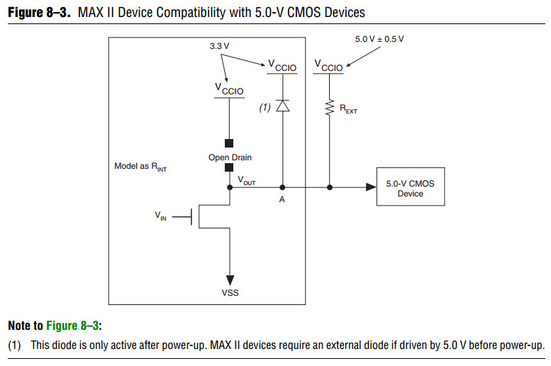
The open-drain pin never drives high, only low or tri-state. When the open-drain pin is active, it drives low.
When the open-drain pin is inactive, the pin is tri-stated and the trace pulls up to 5.0 V by the external resistor.
The purpose of enabling the I/O clamp diode is to protect the MAX II device’s I/O pins.
The 3.3-V VCCIO supplied to the I/O clamp diodes causes the voltage at point A to clamp at 4.0 V,
which meets the MAX II device’s reliability limits when the trace voltage exceeds 4.0 V.
The device operates successfully because a 5.0-V input is within its input specification.
The I/O clamp diode is only supported in the EPM1270 and EPM2210 devices’ I/O Bank 3.
An external protection diode is needed for other I/O banks in EPM1270 and EPM2210 devices
and all I/O pins in EPM240 and EPM570 devices.
The pull-up resistor value should be small enough for sufficient signal rise time,
but large enough so that it does not violate the IOL (output low) specification of MAX II devices.
The maximum MAX II device IOL depends on the programmable drive strength of the I/O output.
Table 8–1 shows the programmable drive strength settings
that are available for the 3.3-V LVTTL/LVCMOS I/O standard for MAX II devices.
The Quartus II software uses the maximum current strength as the default setting.
The PCI I/O standard is always set at 20 mA with no alternate setting.

To compute the required value of REXT, first calculate the model of the open-drain
transistors on the MAX II device. This output resistor (REXT) can be modeled by
dividing VOL by IOL (REXT = VOL/IOL). Table 8–2 shows the maximum VOL for the 3.3-V
LVTTL/LVCMOS I/O standard for MAX II devices.
f For more information about I/O standard specifications, refer to the DC and Switching
Characteristics chapter in the MAX II Device Handbook.

Select REXT so that the MAX II device’s IOL specification is not violated. You can
compute the required pull-up resistor value of REXT by using the equation: REXT =
(VCC/IOL) – RINT. For example, if an I/O pin is configured as a 3.3-V LVTTL with a 16
mA drive strength, given that the maximum power supply (VCC) is 5.5 V, the value of
REXT can be calculated as follows:

This resistor value computation assumes worst-case conditions. You can adjust the
REXT value according to the device configuration drive strength. Additionally, if your
system does not see a wide variation in voltage-supply levels, you can adjust these
calculations accordingly.
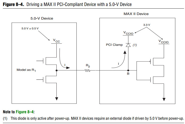
Because MAX II devices are 3.3-V, 32-bit, 66-MHz PCI compliant, the input circuitry
accepts a maximum high-level input voltage (VIH) of 4.0 V.
To drive a MAX II device with a 5.0-V device, you must connect a resistor (R2)
between the MAX II device and the 5.0-V device. See Figure 8–4.
If VCCIO for MAX II devices is 3.3 V and the I/O clamp diode is enabled, the voltage at point B in Figure 8–4 is 4.0 V,
which meets the MAX II devices reliability limits when the trace voltage exceeds 4.0 V.
To limit large current draw from the 5.0-V device, R2 should be small enough for a fast signal rise time
and large enough so that it does not violate the high-level output current (IOH) specifications of the devices driving the trace.
To compute the required value of R2, first calculate the model of the pull-up transistors on the 5.0-V device.
This output resistor (R1) can be modeled by dividing the 5.0-V device supply voltage (VCC) by the IOH: R1 = VCC/IOH
Figure 8–5 shows an example of typical output drive characteristics of a 5.0-V device.
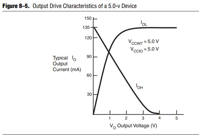
As shown above, R1 = 5.0 V/135 mA.
The values usually shown in data sheets reflect typical operating conditions.
Subtract 20% from the data sheet value for guard band.
This subtraction applied to the above example gives R1 a value of 30.
Select R2 so that the MAX II device’s IOH specification is not violated. For example,
if the above device has a maximum IOH of 8 mA, given the I/O clamp diode,
VIN = VCCIO + 0.7 V = 3.7 V.
Given that the maximum supply load of a 5.0-V device (VCC) is 5.5 V, the value of R2
can be calculated as follows:

This analysis assumes worst-case conditions. If your system does not see a wide
variation in voltage-supply levels, you can adjust these calculations accordingly.
Because 5.0-V device tolerance in MAX II devices requires use of the I/O clamp, and
this clamp is activated only after power-up, 5.0-V signals may not be driven into the
device until it is configured.
The I/O clamp diode is only supported in the EPM1270 and EPM2210 devices’ I/O Bank 3.
An external protection diode is needed for other I/O banks for EPM1270 and EPM2210 devices
and all I/O pins in EPM240 and EPM570 devices.
MAX II Device Compatibility with 5.0-V CMOS Devices的更多相关文章
- Multiplexing SDIO Devices Using MAX II or CoolRunner-II CPLD
XAPP906 Supporting Multiple SD Devices with CoolRunner-II CPLDs There has been an increasing demand ...
- Delphi XE5 Device compatibility
Delphi XE5 Device compatibility https://docs.google.com/spreadsheet/ccc?key=0AoEN2CEsVvJ0dGhVaWJE ...
- 3、一、Introduction(入门):2、Device Compatibility(设备兼容性)
2.Device Compatibility(设备兼容性) Android is designed to run on many different types of devices, from ...
- java.lang.UnsatisfiedLinkError: org.apache.hadoop.util.NativeCrc32.nativeComputeChunkedSumsByteArray(II[BI[BIILjava/lang/String;JZ)V
环境: Spark2.1.0 .Hadoop-2.7.5 代码运行系统:Win 7在运行Spark程序写出文件(savaAsTextFile)的时候,我遇到了这个错误: // :: ERROR U ...
- Android Google官方文档解析之——Device Compatibility
Android is designed to run on many different types of devices, from phones to tablets and television ...
- win7上代码连接hadoop出现错误 :org.apache.hadoop.util.NativeCrc32.nativeComputeChunkedSumsByteArray(II[BI[BIILjava/lang/String;JZ)V
在idea和eclipse中调试hadoop中hdfs文件,之前好好的,结果突然就出现java.lang.UnsatisfiedLinkError: org.apache.hadoop.util.Na ...
- 关于freemarker标签+Spring3.0 V层学习
import标签 就是把其他的ftl页面引用进来 <#import "/common/ui.ftl" as ui> 使用时 <@ui.message/>,m ...
- linux内核挂载根文件系统时报错”VFS: Cannot open root device "ram0" or unknown-block(0,0): error -6“如何处理?
1. 通过error -6得到: #define ENXIO 6 /* No such device or address */ 2. 解决办法 使能CONFIG_BL ...
- VFS: Cannot open root device "nfs" or unknown-block(0,255)错误的解决
1. 解决办法:在内核配置时候文件系统中选中Root file system on NFS
随机推荐
- epoll测试实例
C++ Code 12345678910111213141516171819202122232425262728293031323334353637383940414243444546474849 ...
- CSDN博客专家申请成功
又一个值得纪念的日子,上周六申请CSDN博客专家,今天中午审批通过.使用CSDN好几年了,从未想到能把博客一步步的写到这个地步. 曾经,写过一段博客,只是为了记录和分享.中间由于工作的变动和繁忙中断了 ...
- gtk+学习笔记(七)
今天被一个文本框坑了,基本设置什么的都对,但是就是无法显示中文,按钮名称都可以显示中文,先介绍下文本框的基本函数吧. GtkWidget *gtk_text_view_new(void);新建一个文本 ...
- .net/c#常用框架/中间件简介
任务调度 Quartz.NET:Quartz.NET是一个开源的作业调度框架,非常适合在平时的工作中,定时轮询数据库同步,定时邮件通知,定时处理数据等. Quartz.NET允 许开发人员根据时间间隔 ...
- Pg188-3 构造方法
package org.hanqi.array; public class Father { private String name; private int age; public String g ...
- HashMap 在 Java1.7 与 1.8 中的区别
hashMap 数据结构 如上图所示,JDK7之前hashmap又叫散列链表:基于一个数组以及多个链表的实现,hash值冲突的时候,就将对应节点以链表的形式存储. JDK8中,当同一个hash值(Ta ...
- Django实战(3):Django也可以有scaffold
rails有一个无用的”神奇“功能,叫做scaffold.能够在model基础上,自动生成CRUD的界面. 说它无用,是因为rails的开发者David说,scaffold”不是应用程序开发的目的.它 ...
- Ionic实战九:ionic视频播放
本模板和以前的方式不同,采用的是 iframe方式引入的视频,如下代码:       
- 数据挖掘算法:关联分析二(Apriori)
二.Apriori算法 上文说到,大多数关联规则挖掘算法通常采用的策略是分解为两步: 频繁项集产生,其目标是发现满足具有最小支持度阈值的所有项集,称为频繁项集(frequent itemset). 规 ...
- mysql插入数据时,去掉重复的数据;
1. 利用insert ignore into语句去重 mysql> INSERT IGNORE INTO person_tbl (last_name, first_name) -> VA ...