Spartan-6 FPGA Configuration
These configuration pins serve as the interface for a number of different configuration modes:
• JTAG configuration mode
• Master Serial/SPI configuration mode (x1, x2, and x4)
• Slave Serial configuration mode
• Master SelectMAP/BPI configuration mode (x8 and x16)
• Slave SelectMAP configuration mode (x8 and x16)
The specific configuration mode is selected by setting the appropriate level on the mode
input pins M[1:0]. The M1 and M0 mode pins should be set at a constant DC voltage level,
either through pull-up or pull-down resistors (2.4 kΩ) , or tied directly to ground or
VCCO_2. The mode pins should not be toggled during or before configuration but can be
toggled after.
The terms Master and Slave refer to the direction of the configuration clock (CCLK):
• In Master configuration modes, the Spartan-6 device drives CCLK from an internal
oscillator by default or optional external master clock source GCLK0/USERCCLK. To
select the desired frequency, BitGen -g ConfigRate option is used for the internal
oscillator. The BitGen section of UG628, Command Line Tools User Guide provides more
information.
• In Slave configuration modes, CCLK is an input.
• The JTAG/boundary-scan configuration interface is always available, regardless of the
mode pin settings.
FPGA Configuration Data Source
Spartan-6 FPGAs are designed for maximum flexibility. The FPGA either automatically
loads itself with configuration data from a PROM, or another external intelligent device
like a processor or microcontroller can download the configuration data to the FPGA.
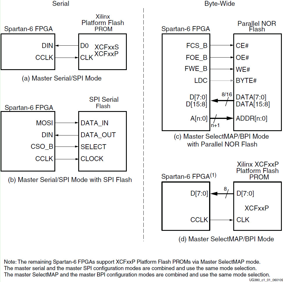
Master Modes
The self-loading FPGA configuration modes, generically called Master modes, as shown in
Figure 1-1. The Master modes leverage various types of nonvolatile memories to store the
FPGA configuration information. In Master mode, the FPGA configuration bitstream
typically resides in nonvolatile memory on the same board, generally external to the
FPGA. The FPGA provides a configuration clock signal called CCLK (the source is from
either an internal oscillator or an optional external master clock source
GCLK0/USERCCLK), and the FPGA controls the configuration process.
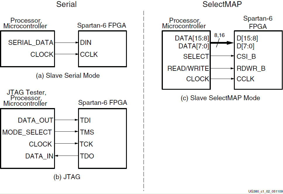
Slave Modes
The externally controlled loading FPGA configuration modes, generically called Slave
modes, are also available with either a serial or byte-wide datapath. In Slave mode, an
external “intelligent agent” such as a processor, microcontroller, DSP processor, or tester
downloads the configuration image into the FPGA, as shown in Figure 1-2. The advantage
of the Slave configuration modes is that the FPGA bitstream can reside almost anywhere in
the overall system. The bitstream can reside in flash, onboard, along with the host
processor's code. It can reside on a hard disk. It can originate somewhere over a network
connection or another type of bridge connection.
The Slave SelectMAP mode is a simple x8- or x16-bit-wide processor peripheral interface,
including a chip-select input and a read/write control input. The Slave Serial mode is
extremely simple, consisting only of a clock and serial data input.
JTAG Connection
The four-wire JTAG interface is common on board testers and debugging hardware. In fact,
the Xilinx programming cables for Spartan-6 FPGAs, listed here, use the JTAG interface for
prototype download and debugging. Regardless of the configuration mode ultimately
used in the application, it is best to also include a JTAG configuration path for easy design
development.
Spartan-6 devices support all the configuration modes supported by the Extended Spartan-3A family.
However, the difference is Spartan-6 devices only expose two mode pins M[1:0],
which define the configuration modes, instead of three mode pins M[2:0] used by the Extended Spartan-3A family.
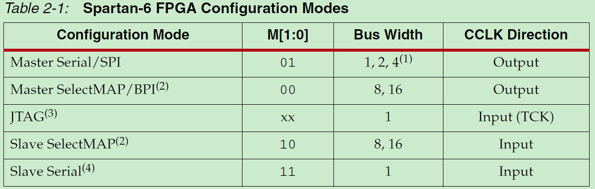
Notes:
1. Utilizing dual and quad SPI modes.
2. Parallel configuration mode bus is auto-detected by the configuration logic.
3. Spartan-6 devices also have a dedicated four-wire JTAG (IEEE Std 1149.1) port
that is always available to the FPGA regardless of the mode pin settings.
4. Default setting due to internal pull-up termination on Mode pins.
JTAG Interface
While there is no specific mode for JTAG, the JTAG interface is available as a configuration
interface any time the device is powered.
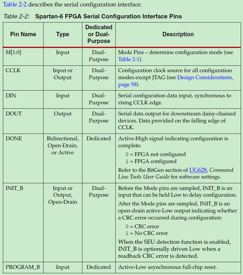
Serial Configuration Interface
In serial configuration modes, the FPGA is configured by loading one configuration bit per CCLK cycle:
• In Master Serial mode, CCLK is an output.
• In Slave Serial mode, CCLK is an input.

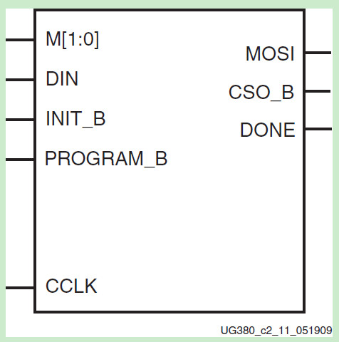
Spartan-6 FPGA Serial Configuration Interface
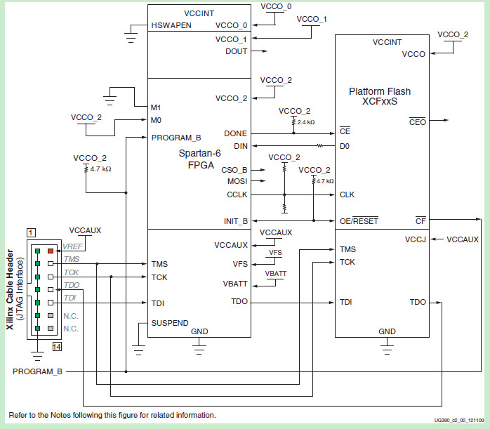
Master Serial
The Master Serial configuration is designed so that the FPGA can be configured from a
Xilinx® Platform Flash PROM, as shown in Figure 2-2.
Notes relevant to Figure 2-2:
1. See Table 5-2, page 66 for internal pin terminations and pins affected by HSWAPEN.
2. DOUT should be connected to the DIN of the downstream FPGA for daisy-chained
configuration modes.
3. The CCLK net requires Thevenin parallel termination. For details, refer to Board
Layout for Configuration Clock (CCLK), page 52.
4. Master Serial and Master SPI are both enabled from the same mode pins. Therefore, the
SPI control pins, CSO_B and MOSI, toggle during configuration.
5. The Spartan-6 FPGA VCCO_2 supply input and the Platform Flash PROM VCCO
supply input must be the same voltage.
6. The DONE pin is by default an open-drain output with an internal pull-up. An
additional external pull-up is recommended. The DONE pin has a programmable
active driver that can be enabled via the BitGen option -g DriveDone.
7. The INIT_B pin is a bidirectional, open-drain pin. An external pull-up resistor is
recommended.
8. The BitGen startup clock setting must be set for CCLK for serial configuration, which
is done by default in the software. See UG628, Command Line Tools User Guide for
details.
9. The PROM in this diagram represents one or more Xilinx PROMs. Multiple Xilinx
PROMs can be cascaded to increase the overall configuration storage capacity, further
described in UG161, Platform Flash PROM User Guide.
10. The BIT file must be reformatted into a PROM file before it can be stored on the Xilinx
PROM. Refer to the Generating PROM Files, page 70, which outlines how to use
iMPACT software to generate the required files.
11. On some Xilinx PROMs, the reset polarity is programmable. RESET should be
configured as active Low when using this setup.
12. Master Serial mode configuration is specific to the Platform Flash XCFS and XCFP
PROM only.
13. Unused configuration pins such as CSI_B and RDWR_B can be left floating or tied to
GND because they are not connected to any configuration logic in this mode. CSI_B
and RDWR_B are dual-purpose pins.
14. VFS is present in XC6SLX75/T, XC6SLX100/T, and XC6SLX150/T devices, and is used
for eFUSE programming. See eFUSE, page 84 for more details.
15. VBATT is present in XC6SLX75/T, XC6SLX100/T, and XC6SLX150/T devices, and is
the power source for AES key storage. If AES encryption is unused, VBATT can be tied
to either VCCAUX or ground, or can be left unconnected.
16. If VCCO_2 is 1.8V, VCCAUX must be 2.5V. If VCCO_2 is 2.5V, VCCAUX can be either 2.5V
or 3.3V.
17. The SUSPEND pin should be Low during power up and configuration. If the Suspend
feature is not used, the SUSPEND pin must be connected to ground.
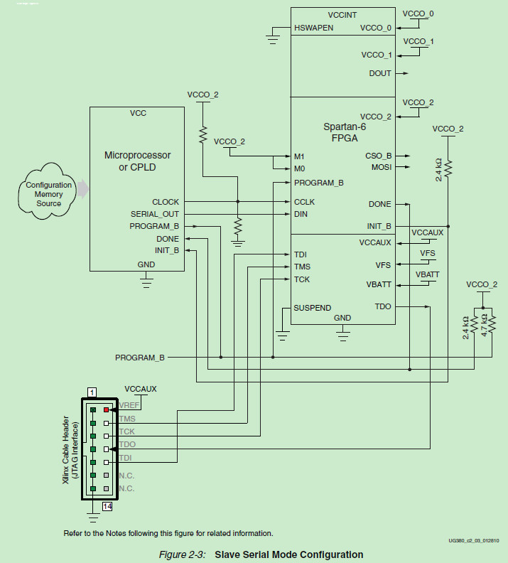
Slave Serial Configuration
Slave Serial configuration is typically used for devices in a serial daisy-chain or when
configuring a single device from an external microprocessor or CPLD (see Figure 2-3).
Design considerations are similar to Master Serial configuration except for the direction of
CCLK. CCLK must be driven from an external clock source, which also provides data (see
Serial Configuration Data Timing, page 27).
Notes relevant to Figure 2-3:
1. See Table 5-2, page 66 for internal pin terminations and pins affected by HSWAPEN.
2. DOUT should be connected to the DIN of the downstream FPGA for daisy-chained
configuration modes.
3. The CCLK net requires Thevenin parallel termination. For more details, see Board
Layout for Configuration Clock (CCLK), page 52.
4. The DONE pin is by default an open-drain output with an internal pull-up. An
additional external pull-up is recommended. The DONE pin has a programmable
active driver that can be enabled via the BitGen option -g DriveDone.
5. The INIT_B pin is a bidirectional, open-drain pin. An external pull-up resistor is
recommended.
6. The SPI control pins, CSO_B and MOSI, toggle during serial configuration.
7. VFS is present in XC6SLX75/T, XC6SLX100/T, and XC6SLX150/T devices, and is used
for eFUSE programming. See eFUSE, page 84 for more details.
8. VBATT is present in XC6SLX75/T, XC6SLX100/T, and XC6SLX150/T devices, and is
the power source for AES key storage. If AES encryption is unused, VBATT can be tied
to ground or can be left unconnected.
9. If VCCO_2 is 1.8V, VCCAUX must be 2.5V. If VCCO_2 is 2.5V, VCCAUX can be either 2.5V
or 3.3V.
10. The SUSPEND pin should be Low during power up and configuration. If the Suspend
feature is not used, the SUSPEND pin must be connected to ground.
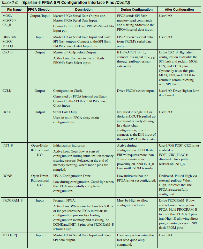
SPI Configuration Interface
The Master Serial Peripheral Interface (SPI) (Figure 2-11) allows a SPI serial flash to be used
to store configuration data. The Spartan-6 FPGA configures itself from a directly attached
industry-standard SPI serial flash PROM. Although SPI is a standard four-wire interface,
various available SPI flash memories use different read commands and protocol.
Figure 2-12 shows the connections for an SPI configuration with a data width of x1 or x2.
These connections are the same because the x2 flash devices use the D pin as a dual
purpose Data In/Out pin. Connections for the SPI x4 option are shown in Figure 2-13,
page 41; two additional data pins provide a 4-bit data interface. Daisy-chained
configuration mode is only available in SPI x1 mode. The FPGA pin connections to the SPI
flash PROM involved in the Master SPI mode are listed in Table 2-5.
The iMPACT programming software provides the ability to program an SPI serial flash
using an indirect programming method. This downloads a new FPGA design that
provides a connection from the iMPACT software through the Spartan-6 device to the SPI
flash. Previous FPGA memory contents are lost. For a list of supported SPI flash devices,
refer to the ISE® software overview at
http://www.xilinx.com/support/documentation/sw_manuals/xilinx11/isehelp_start.htm and
navigate to the iMPACT help section called “Introduction to Indirect Programming – SPI
or BPI Flash Memory”.
For more details see XAPP974: Indirect Programming of SPI Serial Flash PROMs with
Spartan-3A FPGAs.

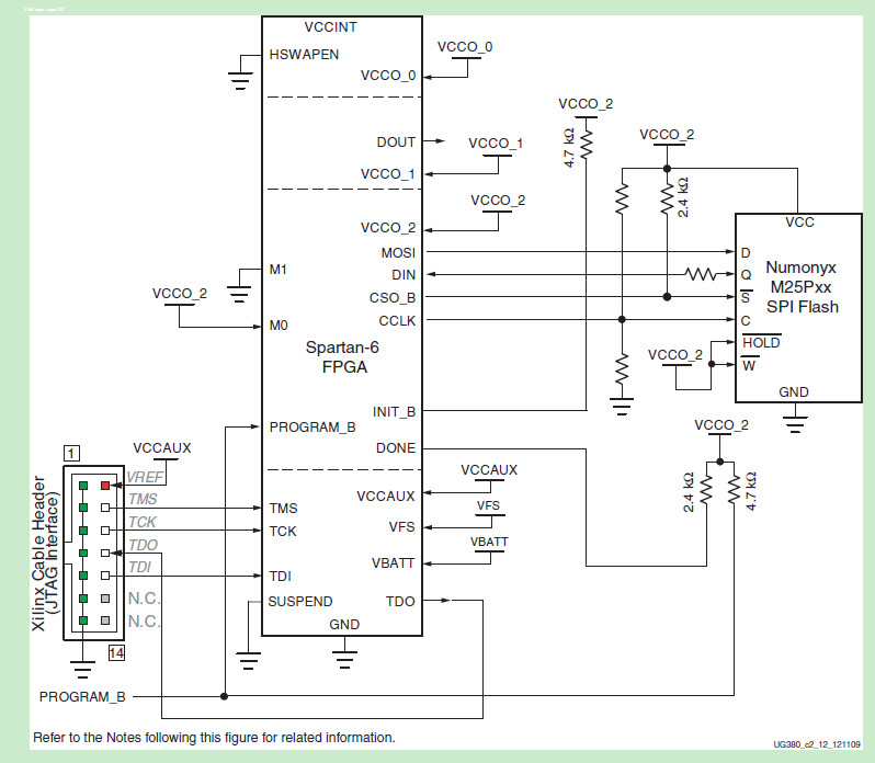
Notes relevant to Figure 2-12:
1. See Table 5-2, page 66 for internal pin terminations and pins affected by HSWAPEN.
2. DOUT should be connected to the DIN of the downstream FPGA for daisy-chained
configuration modes.
3. For more details on CCLK termination, see Board Layout for Configuration Clock
(CCLK), page 52.
4. A series resistor should be considered for the datapath from the flash to the FPGA to
minimize overshoot. The proper resistor value can be determined from simulation.
5. The Spartan-6 FPGA VCCO_2 supply must be the same voltage as VCC of the SPI
device.
6. CSO_B and MOSI are clocked by the CCLK falling edge.
7. DIN is clocked on the rising edge of the CCLK.
8. There are additional pins on the SPI flash side, such as Write Protect and Hold. These
pins are not used in FPGA configuration (read only). But they should be tied off
appropriately according to the SPI vendor’s specification.
9. If HSWAPEN is left unconnected or tied High, a pull-up resistor is required for CSO_B.
10. The CCLK frequency is adjusted by using the BitGen option ConfigRate if the source
is the internal oscillator. If an external source is used, see External Configuration Clock
for Master Modes, page 51 for more details.
11. The DONE pin is by default an open-drain output with an internal pull-up. An
additional external pull-up is recommended. The DONE pin has a programmable
active driver that can be enabled via the BitGen option -g DriveDone.
12. When the digital clock manager (DCM) or PLL lock wait is enabled before the DONE
release cycle during startup, the FPGA continues to clock in data until the startup wait
condition is met and DONE is released. See Required Data Spacing between MultiBoot
Images, page 128 for considerations specific to MultiBoot Configuration.
13. Figure 2-12 shows a Numonyx SPI flash device. Refer to the ISE software overview at
http://www.xilinx.com/support/documentation/sw_manuals/xilinx11/isehelp_start.htm
and navigate to the iMPACT help documentation (“Introduction to Indirect
Programming”) to see which devices are supported for indirect SPI configuration
using iMPACT.
14. VFS is present in XC6SLX75/T, XC6SLX100/T, and XC6SLX150/T devices, and is used
for eFUSE programming. See eFUSE, page 84 for more details.
15. VBATT is present in XC6SLX75/T, XC6SLX100/T, and XC6SLX150/T devices, and is
the power source for AES key storage. If AES encryption is unused, VBATT can be tied
to ground or can be left unconnected.
16. If VCCO_2 is 1.8V, VCCAUX must be 2.5V. If VCCO_2 is 2.5V, VCCAUX can be either 2.5V
or 3.3V.
17. The SUSPEND pin should be Low during power up and configuration. If the Suspend
feature is not used, the SUSPEND pin must be connected to ground.
Spartan-6 FPGAs also support x4 configuration
with SPI PROMs in Master Serial Mode.

Notes relevant to Figure 2-13:
1. The connection shown in Figure 2-13 uses the Winbond W25Q SPI series flash PROM.
To enable the Quad output operation, the user must set the QE bit of the PROM’s
status_reg[9] to 1 before the device can transmit in quad output mode, which is done
at programming time in iMPACT software.
2. CCLK can be provided by the FPGA or an external clock source.
3. There are default pull-ups on the PROGRAM_B, INIT_B, and M0 pin.
4. Software support for x4 requires the x4 capability enabled in BitGen.
5. The SPI device needs to be programmed with a specific register setting, which can be
done in iMPACT software, to enable x4 output.
Master SPI Dual (x2) and Quad (x4) Read Commands
The Master SPI configuration mode in Spartan-6 FPGAs supports the Winbond W25Q
Quad I/O SPI flash memory dual (x2) and quad bit (x4) memory read commands. To
enable this configuration method in software, the BitGen spi_buswidth option is used to
create a .bit file for SPI x2 or x4.
The FPGA still initially boots in x1 mode and then switches to x2 or x4 mode.
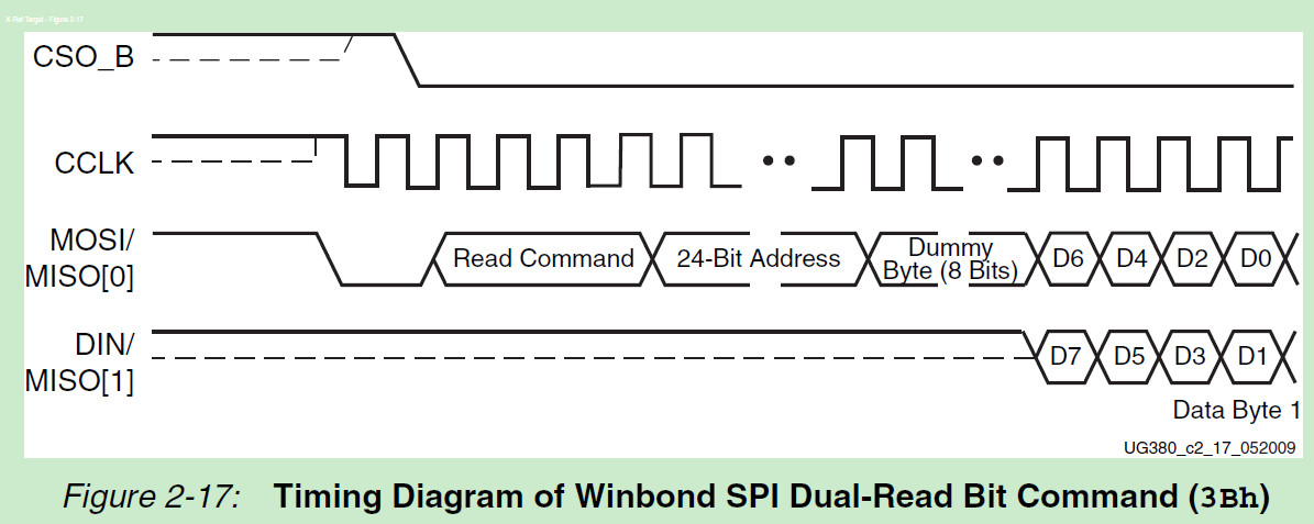
In x2 mode, the Fast-Read Dual Output (3Bh) instruction is issued and is similar to the
standard Fast Read (0Bh) instruction except that data is output on two pins, DO and DIO
(MOSI), instead of just DO. This allows data to be transferred from the dual output at twice
the rate of standard SPI devices. The timing diagram of the Master Serial SPI configuration
mode using the Winbond SPI flash with dual read-bit command (3Bh) is shown in
Figure 2-17.
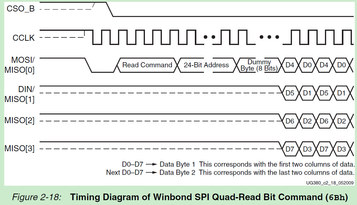
In x4 mode, the Fast-Read Quad Output (6Bh) instruction is issued and is similar to the
standard Fast Read (0Bh) instruction except that data is output on four data pins, instead
of just DO. This allows data to be transferred from the quad output at four times the rate of
standard SPI devices. The timing diagram of the Master Serial SPI configuration mode
using the Winbond SPI flash with quad read bit command (6Bh) is shown in Figure 2-18.
Spartan-6 FPGA Configuration的更多相关文章
- Xilinx Zynq FPGA Boards板
Xilinx Zynq FPGA Boards板 Xilinx Zynq FPGA Boards 介绍 Styx是一个易于使用的Zynq开发模块,具有Xilinx的Zynq ZC7020 SoC和FT ...
- 关于Xilinx FPGA JTAG下载时菊花链路中的芯片数量
关于Xilinx FPGA JTAG下载时菊花链路中的芯片数量 emesjx | 2014-08-13 13:13:30 阅读:1793 发布文章 当一个系统中含有多片(2片以上)Xil ...
- 如何保证FPGA PCIe唤醒能满足PC的100ms 的时间要求(Autonomous Mode)?
原创By DeeZeng [ Intel FPGA笔记 ] PC 需要PCIe设备在 100ms 内启动,这样PC 才能扫描到PCIe 设备.对于 FPGA PCIe 板卡,同样也需要满足这个时间要 ...
- 基于FPGA Manager的Zynq PL程序写入方案
本文主要描述了如何在Linux系统启动以后,在线将bitstream文件更新到ZYNQ PL的过程及方法.相关内容主要译自xilinx-wiki,其中官网给出了两种方法,分别为Device Tree ...
- 如何为应用选择最佳的FPGA(下)
如何为应用选择最佳的FPGA(下) How to select an FPGA board? FPGA板的选择在很大程度上受FPGA本身的影响,也受整个板的特性和性能的影响.们已经在上面的章节中讨论了 ...
- XuLA/XuLA2
http://www.xess.com/prods/prod048.php XuLA http://www.xess.com/prods/prod055.php XuLA2 http://www.xe ...
- Papilio Pro Boards
http://papilio.cc/index.php?n=Papilio.PapilioOne The Papilio is an Open Source FPGA development boar ...
- 如何为编程爱好者设计一款好玩的智能硬件(三)——该选什么样的MCU呢?
一.我的构想:如何为编程爱好者设计一款好玩的智能硬件(一)——即插即用.积木化.功能重组的智能硬件模块构想 二.别人家的孩子:如何为编程爱好者设计一款好玩的智能硬件(二)——别人是如何设计硬件积木的! ...
- linux内核更新前后配置文件的比较
说明:这里先给出一个比较的结果,作为记录,后续会给出内核配置差异的详细解释. [root@xiaolyu linux-4.7.2]# diff .config .config_bak 3c3< ...
随机推荐
- ubuntu无法获得锁 /var/lib/dpkg -open 问题
问题: 方法: sudo rm /var/lib/dpkg/lock 然后再安装就可以了
- js固定小数位数 .toFixed()
toFixed(num)法可把 Number 四舍五入为指定小数位数的数字. num为需要固定的位数 var num=2;console.log(num.toFixed(2));//2.00;var ...
- oracle造成系统CPU过高的检查sql
1. 根据占用CPU高的进程号来查询这个进程执行的SQL语句: CPU过高的进程号: #首先找到CPU过高的进程号 # top -bn1 是静态找到占用最高的进程 [root@localhost ~] ...
- hdu 5895(矩阵快速幂+欧拉函数)
题目链接:http://acm.hdu.edu.cn/showproblem.php?pid=5895 f(n)=f(n-2)+2*f(n-1) f(n)*f(n-1)=f(n-2)*f(n-1)+2 ...
- 教你如何更改android应用的包名
Android 源码自带了很多应用程序,想改个包名方便修改?很简单,两步搞定,以packages/apps/Settings为例: 1.打开AndroidManifest.xml,把 <mani ...
- PHP 权威代码风格规范
1.常规 尽量统一ide 比如phpstream 配置文件(Settings → Code Style → PHP → Set from... → Predefined Style → PSR1/PS ...
- JavaScript中变量、作用域、内存问题
这几天,闲的没事看看JavaScript高级编程,感觉JavaScript真的很强大,尤其是采用面向对象的编程方式. 一. 基本类型和引用类型的值: ECMAScript变量可能包含两种不同数据类 ...
- mysql左连接,右连接,内连接
- Xamarin 2017.9.19更新
Xamarin 2017.9.19更新 本次更新是添加Xamarin.iOS对iOS 11和Xcode 9的支持.Visual Studio 2017升级到15.3.5获得更新功能.Visual ...
- Failed to add VMware DC to zone due to : This DC is being managed by other CloudStack deployment.
1.下载VMware-PowerCLI 2.安装VMware-PowerCLI 安装过程中会重复重启,请确认重启,不要设置稍后手动重启. 3.在开始,菜单中选择 vmware ->VMware ...